Sensor semiconductor device and manufacturing method thereof

a technology of semiconductor devices and manufacturing methods, applied in semiconductor/solid-state device manufacturing, semiconductor devices, electrical equipment, etc., can solve the problems of affecting and affecting the alignment of slant grooves to be formed, so as to improve the reliability of traces

Inactive Publication Date: 2008-08-21
SILICONWARE PRECISION IND CO LTD
View PDF2 Cites 17 Cited by
  • Summary
  • Abstract
  • Description
  • Claims
  • Application Information

AI Technical Summary

Benefits of technology

[0014]The manufacturing method for a sensor semiconductor device of the present invention essentially comprises: providing a wafer having a plurality of sensor chips, forming a plurality of grooves between bond pads on active surfaces of the adjacent sensor chips; forming conductive traces in the grooves for electrically connecting the bond pads on the active surfaces of the adjacent sensor chips; mounting a transparent medium on the wafer for covering sensing areas of the sensor chips; and thinning the sensor chips from the non-active surfaces down to the grooves, thereby exposing the conductive traces from the non-active surfaces. By contrast, it is disclosed in the prior art that the extension traces and the adhesive layer are formed in the non-active surfaces of the sensor chips (that is, the back of the wafer) and electrically connected to the bond pads of the sensor chips, and slanted grooves are formed down to the glass; and the metal routing traces are formed on the slanted grooves and a portion of the covered layer adjacent to the slanted grooves and electrically connected to the extension traces. Owing to an acute angle formed on the contact between the metal routing traces formed at the flanks of the sensor semiconductor device and the extension traces of the bond pads on top of the chips, the contact may crack due to the st

Problems solved by technology

There is an acute angle of contact between the metal routing traces formed at the flanks of the sensor semiconductor device and the extension traces of the bond pads on top of the chips, and thus the contact is likely to sever due to stress concentration.
Moreover, it is the back of the wafer where the slanted grooves are formed during the manufacturing process, alignment of the slanted grooves to be formed is so difficult as to prevent connection of the metal routing traces and exte

Method used


Image

  • Sensor semiconductor device and manufacturing method thereof
  • Sensor semiconductor device and manufacturing method thereof
  • Sensor semiconductor device and manufacturing method thereof

Examples


Embodiment Construction

[0018]The following specific embodiments are provided to illustrate the present invention. Persons skilled in the art can readily gain insight into other advantages and features of the present invention based on the contents disclosed in this specification.

[0019]FIGS. 2A to 2I are schematic views showing the first preferred embodiment of a sensor semiconductor device and a manufacturing method thereof in accordance with the present invention. Mass production of the sensor semiconductor device of the present invention is described as follows.

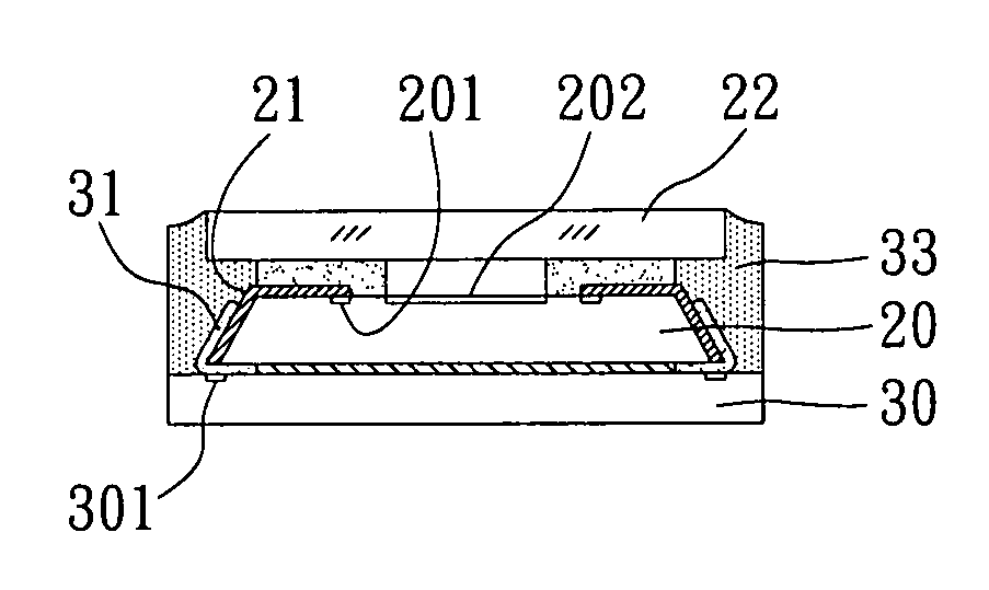
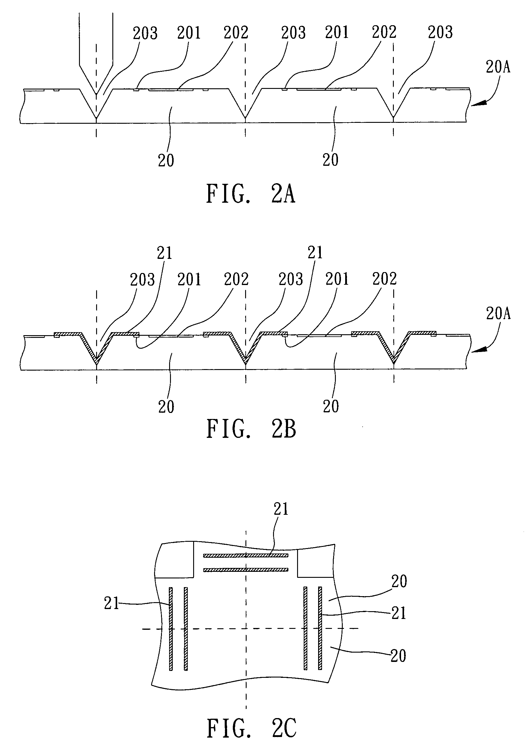
[0020]Referring to FIG. 2A, a wafer 20A having a plurality of sensor chips 20 is provided, wherein each of the sensor chips 20 has an active surface and a non-active surface opposite thereto, a sensing area 202 and a plurality of bond pads 201 are provided on the active surfaces, and a plurality of grooves 203 are formed between the bond pads 201 on the active surfaces of adjacent ones of the sensor chips 20. The cross-section of the grooves 203 ...


PUM


Abstract

This invention discloses a sensor semiconductor device and a manufacturing method thereof, including: providing a wafer having a plurality of sensor chips, forming a plurality of grooves between bond pads on active surfaces of the adjacent sensor chips; forming conductive traces in the grooves for electrically connecting the bond pads; mounting a transparent medium on the wafer for covering sensing areas of the sensor chips; thinning the sensor chips from the non-active surfaces down to the grooves, thereby exposing the conductive traces; cutting the wafer to separate the sensor chips; mounting the sensor chips on a substrate module having a plurality of substrates, electrically connecting the conductive traces to the substrates; providing an insulation material on the substrate module and between the sensor chips so as to encapsulate the sensor chips but expose the transparent medium; and cutting the substrate module to separate a plurality of resultant sensor semiconductor devices.

Description

BACKGROUND OF THE INVENTION[0001]1. Field of the Invention[0002]The present invention relates to sensor semiconductor devices and manufacturing methods thereof, and more particularly, to a wafer-level chip-scale packaged (WLCSP) sensor semiconductor device and a manufacturing method thereof.[0003]2. Description of the Prior Art[0004]It is known in the art that image sensor packaging involves mounting a sensor chip on a chip carrier element, electrically connecting the sensor chip and the chip carrier element by means of bonding wires, covering the upper surface of the sensor chip with glass, thereby allowing image light to be retrieved by the sensor chip. Afterward, at a system factory the fully packaged image sensor package is integrated into an external device, such as a printed circuit board (PCB), for use in digital still cameras (DSC), digital video cameras (DV), optical mouses, cellular phones, etc. Owing to ever-increasing information transmission capacity, miniaturization of...

Claims


Application Information

Patent Timeline
IPC IPC(8): H01L31/0203H01L31/18
CPCH01L21/78H01L27/14618H01L2224/94H01L31/0203H01L27/14687
Inventor CHAN, CHANG-YUEHHUANG, CHIEN-PINGCHANG, TSE-WENHUANG, CHIH-MINGHSIAO, CHENG-HSU
Owner SILICONWARE PRECISION IND CO LTD
Why Eureka
Try Eureka