
Beol interconnect structures with improved resistance to stress

Inactive Publication Date: 2008-08-21
TAIWAN SEMICON MFG CO LTD
View PDF9 Cites 47 Cited by
  • Summary
  • Abstract
  • Description
  • Claims
  • Application Information

AI Technical Summary

Benefits of technology

[0006]In accordance with an aspect of the invention, a chip is provided which includes a back-end-of-line (“BEOL”) interconnect structure. The BEOL interconnect structure includes a plurality of interlevel dielectric (“ILD”) layers which include a dielectric material curable by ultraviolet (“UV”) radiation. A plurality of metal interconnect wiring layers are embedded in the plurality of ILD layers. Dielectric barrier layers cover the plurality of metal interconnect wiring layers, the dielectric barrier layers being adapted to reduce diffusion of materials between the metal interconnect wiring layers and the ILD layers. One of more of the dielectric barrier layers is adapted to retain compressive stress while withstanding UV radiation sufficient to cure the dielectric material of the ILD layers, making the BEOL structure better capable of avoiding deformation due to thermal and / or mechanical stress.

Problems solved by technology

Under certain circumstances, chips may be subjected to external stresses, either during the manufacture or packaging of the chips, or when the packaged chips are mounted or installed in an electronic system for use.
Occasionally, such stresses can cause cracking and delamination of dielectric and metal films therein.
Difficulties lie in finding appropriate materials and manufacturing processes which permit copper metal lines to be utilized in certain types of low-K ILD materials, particularly when high stress conditions are present after UV processing.

Method used


Image

  • Beol interconnect structures with improved resistance to stress
  • Beol interconnect structures with improved resistance to stress
  • Beol interconnect structures with improved resistance to stress

Examples


Embodiment Construction

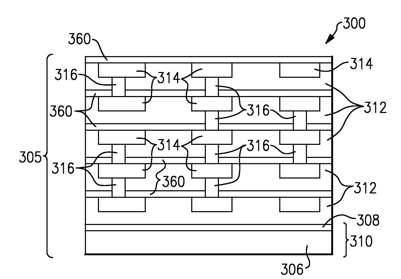
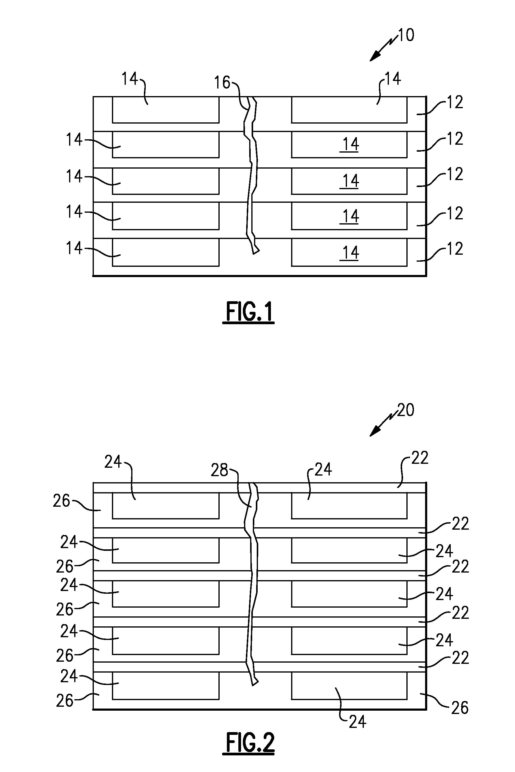
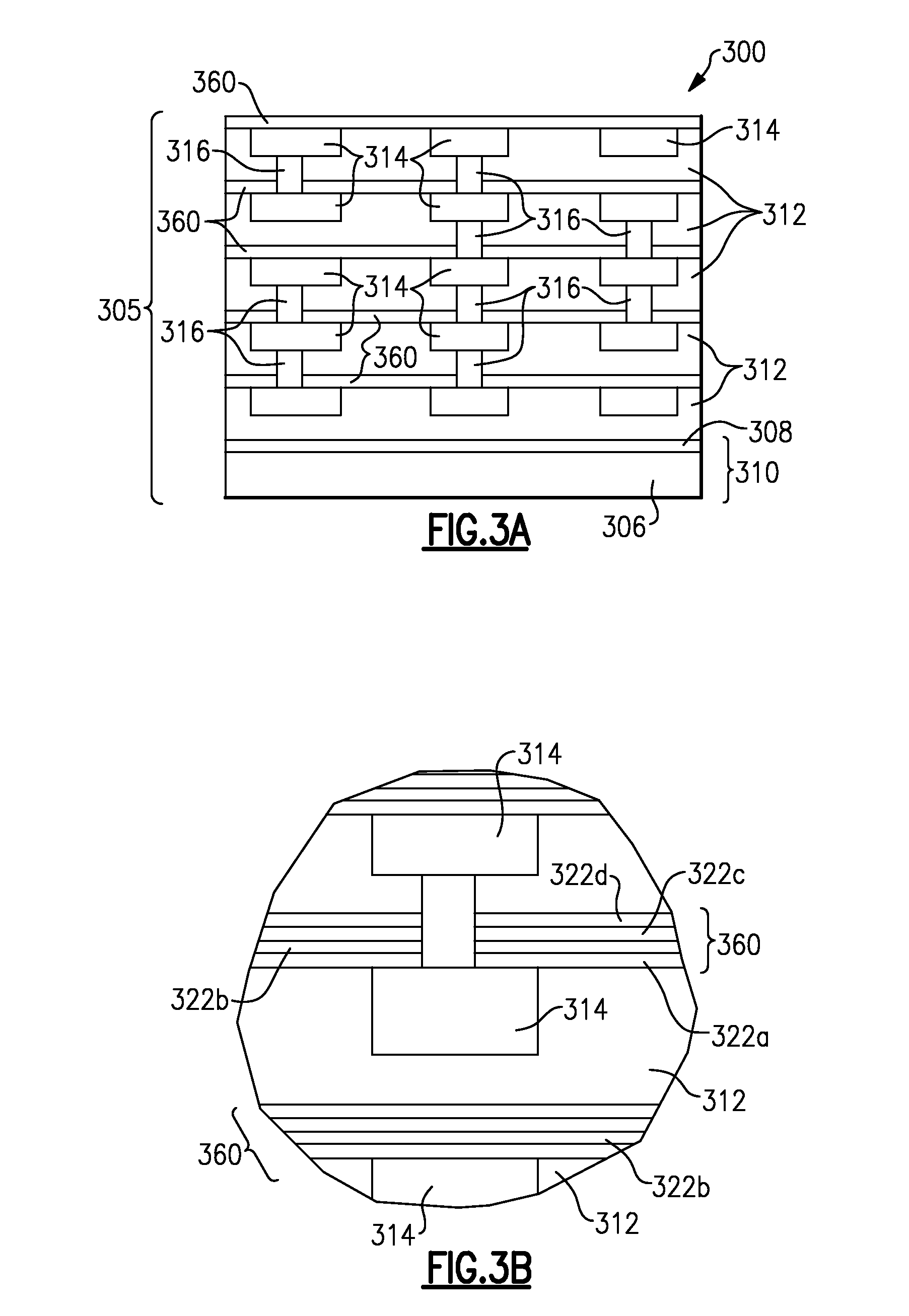
[0014]Certain low dielectric constant (“low-K”) low-K ILD materials, e.g., SiCOH, are best cured using UV radiation, or require ultraviolet (“UV”) to cure. Exposure to UV radiation can cause the properties of materials utilized in a BEOL interconnect structure to change. Sometimes, such changes can lead to defects in the BEOL interconnect structure which might appear later after the chip has undergone stresses attendant with long-term use.

[0015]To test the long-term reliability of a BEOL interconnect structure having a UV-cured low-K dielectric, the inventors modeled the effects of thermal cycling stress upon a BEOL interconnect structure 10 similar to that shown in FIG. 1. As shown in FIG. 1, the model BEOL interconnect structure 10 includes a series of low-K ILD material layers 12, each including a dielectric material such as porous SiCOH, for example. Embedded within each ILD layer 12 is a metal wiring interconnect layer 14. When SiCOH is exposed to UV radiation, it tends to acqu...


PUM


Abstract

A chip is provided which includes a back-end-of-line (“BEOL”) interconnect structure. The BEOL interconnect structure includes a plurality of interlevel dielectric (“ILD”) layers which include a dielectric material curable by ultraviolet (“UV”) radiation. A plurality of metal interconnect wiring layers are embedded in the plurality of ILD layers. Dielectric barrier layers cover the plurality of metal interconnect wiring layers, the dielectric barrier layers being adapted to reduce diffusion of materials between the metal interconnect wiring layers and the ILD layers. One of more of the dielectric barrier layers is adapted to retain compressive stress while withstanding UV radiation sufficient to cure the dielectric material of the ILD layers, making the BEOL structure better capable of avoiding deformation due to thermal and / or mechanical stress.

Description

BACKGROUND OF THE INVENTION[0001]The present invention relates to semiconductor devices, and more particularly, to back-end-of-line (BEOL) interconnect structures.[0002]Integrated circuits typically include a plurality of semiconductor devices and interconnect wiring. Networks of metal interconnect wiring typically connect the semiconductor devices from above the semiconductor portion of the substrate. Multiple levels of metal interconnect wiring above the semiconductor portion of the substrate are connected together to form a back-end-of-line (“BEOL”) interconnect structure. Within such structure, metal lines run parallel to the substrate and conductive vias run perpendicular to the substrate, the conductive vias interconnecting the different levels of metal wiring lines.[0003]Two developments contribute to increased performance of contemporary integrated circuits. One of them is the use of copper as the interconnect metal in BEOL interconnect structures, due to the higher conducti...

Claims


Application Information

Patent Timeline
IPC IPC(8): H01L23/52H01L21/00
CPCH01L21/76822H01L21/76826H01L21/76832H01L23/53295H01L21/76835H01L23/5329H01L21/76834H01L2924/0002H01L2924/00H01L21/3205
Inventor RESTAINO, DARRYL D.BONILLA, GRISELDADIMITRAKOPOULOS, CHRISTOS D.GATES, STEPHEN M.KIM, JAE H.LANE, MICHAEL W.LIU, XIAO H.NGUYEN, SON V.SHAW, THOMAS M.WIDODO, JOHNNY
Owner TAIWAN SEMICON MFG CO LTD
Features
  • Generate Ideas
  • Intellectual Property
  • Life Sciences
  • Materials
  • Tech Scout
  • Unparalleled Data Quality
  • Higher Quality Content
  • 60% Fewer Hallucinations
Learn More