
Method for operating a vacuum Coating apparatus
- Summary
- Abstract
- Description
- Claims
- Application Information
AI Technical Summary
Benefits of technology
Problems solved by technology
Method used
Image

Examples
Embodiment Construction
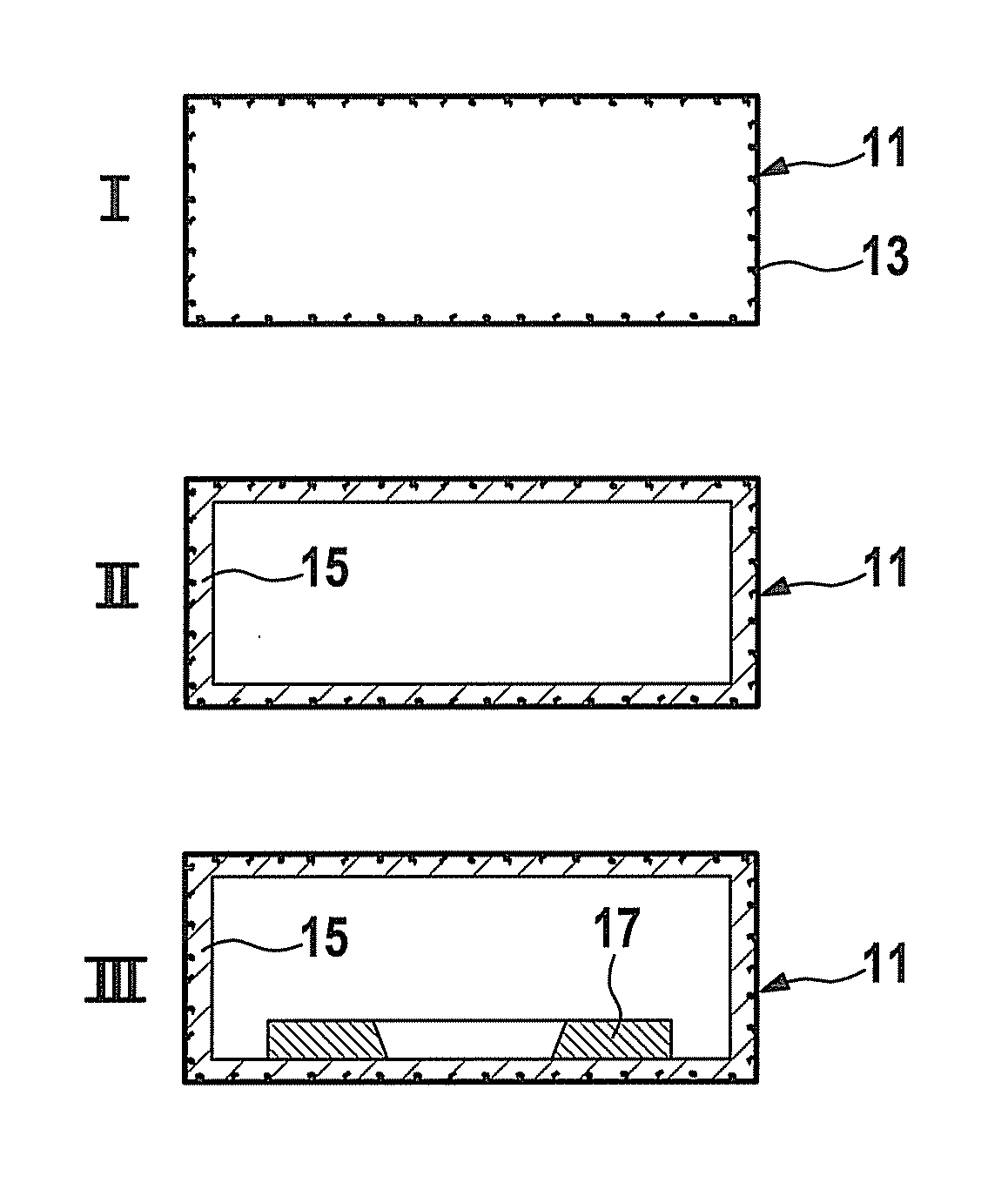
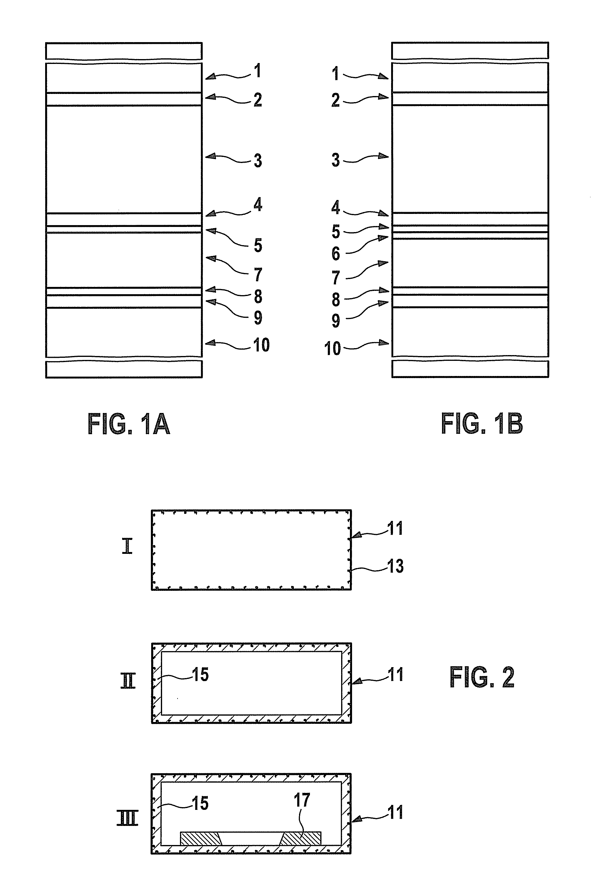
[0020]FIG. 2 schematically shows a cross-section of the interior of a coating chamber 11 in three phases of an operating method according to the present invention. In phase I, after a step of cleaning the chamber with gas containing fluorine, residues 13 are situated on and in the walls. In phase II, accomplished through a PECVD deposition step without substrates, a diffusion blocking layer 15 is situated on the entire inner wall of coating chamber 11. This blocking layer completely covers all residues still present in phase I, and prevents their diffusion into the interior of the chamber.
[0021]In phase III, a substrate 17 for solar cell production is situated in coating chamber 11, which is completely lined with diffusion blocking layer 15, and this substrate is exposed to conventional coating steps. After one or more depositions of layers containing silicon, a cleaning step is again carried out using gas containing fluorine, and diffusion blocking layer 15 is removed in this step ...
PUM
| Property | Measurement | Unit |
|---|---|---|
| Thickness | aaaaa | aaaaa |
| Thickness | aaaaa | aaaaa |
| Thickness | aaaaa | aaaaa |
Abstract
Description
Claims
Application Information