Method of forming two-dimensional pattern by using nanospheres
- Summary
- Abstract
- Description
- Claims
- Application Information
AI Technical Summary
Benefits of technology
Problems solved by technology
Method used
Image

Examples
Embodiment Construction
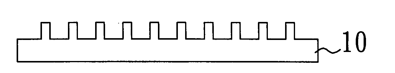
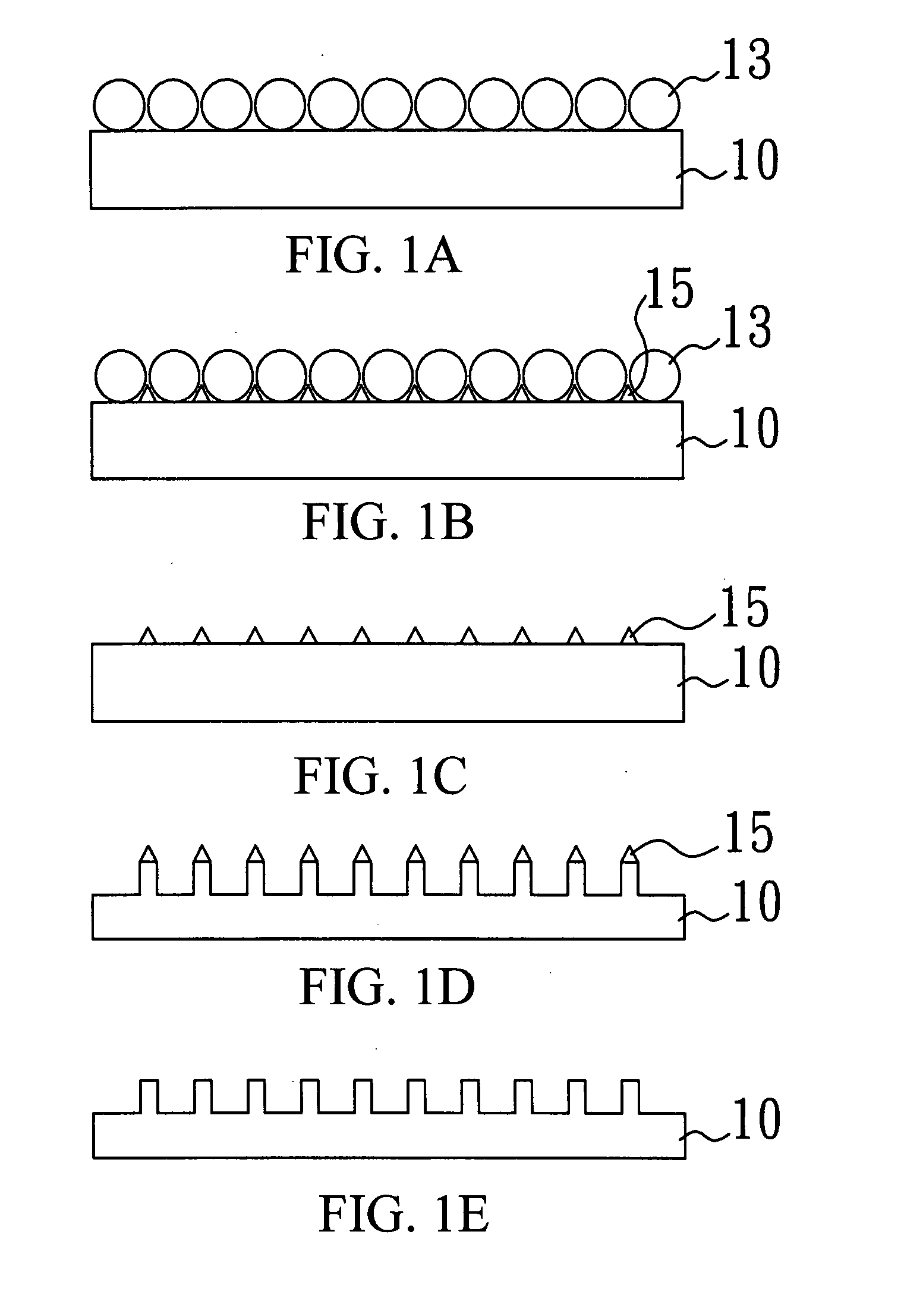
[0023]FIGS. 1A to 1E are schematic views of a method of forming a two-dimensional pattern (e.g., a photonic crystal pattern) on a surface of a photoelectric element substrate according to a first preferred embodiment of the present invention. The photoelectric element provided by the present invention can be an LED or a semiconductor laser. Firstly, as shown in FIG. 1A, a plurality of nanospheres 13 is closely arranged on a substrate 10 of the photoelectric element, and the material of the substrate 10 can be sapphire, SiC, Si, metal (e.g., Cu, Ag, Al), AlN, GaN, GaAs, AlInGaP or diamond with an epitaxial structure of the photoelectric element. Next, as shown in FIG. 1B, a metal material 15 is deposited among the spheres to act as the mask, and then, the nanospheres 13 are removed (as shown in FIG. 1C). Then, the RIE is preformed by using the mask (as shown in FIG. 1D). Finally, the metal material 15 is removed to form the two-dimensional pattern as shown in FIG. 1E on the substrate...
PUM
 Abstract
Description
Claims
Application Information
 - Generate Ideas
- Intellectual Property
- Life Sciences
- Materials
- Tech Scout
- Unparalleled Data Quality
- Higher Quality Content
- 60% Fewer Hallucinations
Browse by: Latest US Patents, China's latest patents, Technical Efficacy Thesaurus, Application Domain, Technology Topic, Popular Technical Reports.
© 2025 PatSnap. All rights reserved.Legal|Privacy policy|Modern Slavery Act Transparency Statement|Sitemap|About US| Contact US: help@patsnap.com