Method of forming composite opening and method of dual damascene process using the same

a damascene and composite opening technology, applied in the field of semiconductor/solid-state device manufacturing, basic electric elements, electrical apparatus, etc., can solve the problems of difficult copper patterning, electrical problems of elements, and the reliability of elements

Active Publication Date: 2008-08-21
UNITED MICROELECTRONICS CORP
View PDF5 Cites 2 Cited by
  • Summary
  • Abstract
  • Description
  • Claims
  • Application Information

AI Technical Summary

Benefits of technology

[0009]Accordingly, the present invention is directed to provide a method of fabricating a dual damascene structure, in which the corner of a trench can be prevented from being rounded and also the bridging of two neighboring dual damascene structures can be overcome.
[0010]The present invention is also directed to provide a method of fabricating the dual damascene structure, in which the forming of a fence-shaped dielectric layer can be prevented.
[0011]The present invention is further directed to provide a method of forming a composite opening, in which the corner of a wide opening can be prevented from being rounded and the forming of a fence at the corner of the narrow opening can be prevented.
[0033]The method of fabricating the dual damascene structure of the present invention can prevent the corner of the trench from being rounded, prevent the two neighboring dual damascene structures from being bridged, and prevent the forming of the fence-shaped dielectric layer at the corner of the via opening.
[0034]The method of forming the composite opening of the present invention can prevent the corner of the wide opening from being rounded and prevent the corner of the narrow opening from forming the fence-shaped bump.

Problems solved by technology

However, as it is difficult to pattern the copper in the conventional photolithographic etching technique, a dual damascene process has been developed.
When the method of forming the via opening first and then forming the trench is employed in the dual damascene process, in the etching process of forming the trench, the corresponding metal layer under the via opening may be damaged by etching, thus causing the electrical problem of elements.
However, in the method, usually because of the shadowing effect of the gap fill material 112, after the trench 120 is formed in the subsequent etching, a dielectric layer 106a with a fence shape is left at a corner 110a of the via opening 110, thus causing the problem of the reliability of elements.
However, it is quite difficult to eliminate the fence-shaped dielectric layer.
However, under the influence of uniformity of etching and micro-loading effect, the thicknesses of the gap fill material at the center of the substrate and at the edge of the substrate, or the thicknesses of the gap fill material in a dense region and in a loose region of the substrate are greatly different, such that the process window is very narrow.

Method used


Image

  • Method of forming composite opening and method of dual damascene process using the same
  • Method of forming composite opening and method of dual damascene process using the same
  • Method of forming composite opening and method of dual damascene process using the same

Examples


first embodiment

The First Embodiment

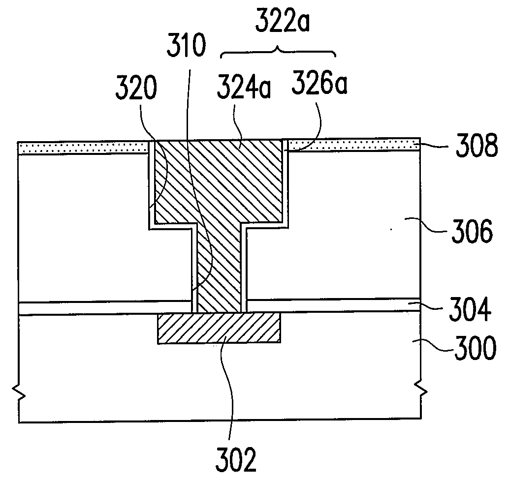
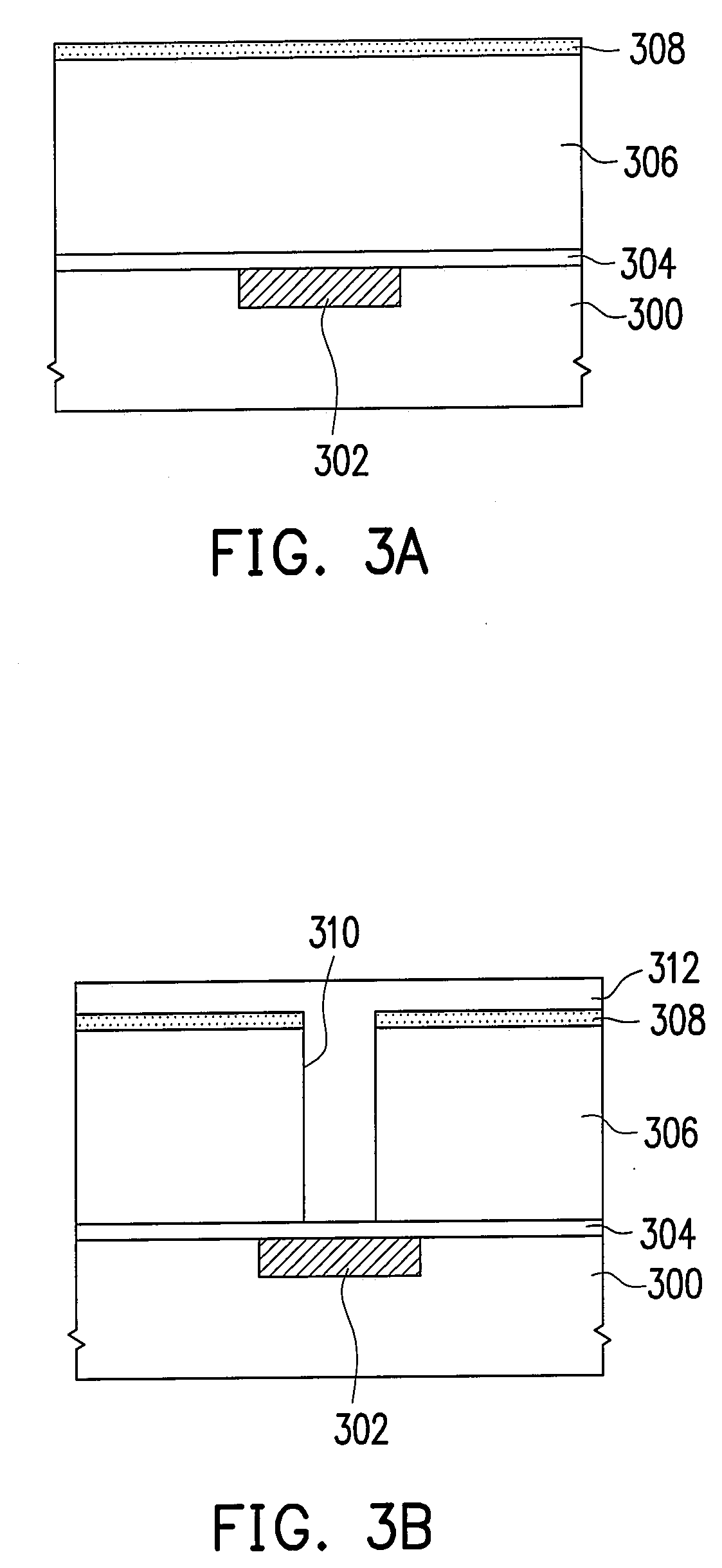
[0040]Referring to FIG. 3A, the dual damascene structure of this embodiment is formed on a substrate 300. A conductive layer 302 is already formed on the substrate 300, and a liner 304 is already covered on the conductive layer 302. The substrate 300 is, for example, a semiconductor substrate, such as a silicon substrate or a silicon-on-insulator (SOI) substrate. The conductive layer 302 is, for example, a metal interconnect, such as a copper wire. The liner 304 covered on the conductive layer 302 can be used to prevent the conductive layer 302 from being oxidized, the material thereof is, for example, a layer of SiN, and the forming method is, for example, chemical vapor deposition (CVD). A dielectric layer 306 is formed on the liner 304, and the material thereof is, for example, a low dielectric constant material. The low dielectric constant material is a material layer with a dielectric constant lower than 4, for example fluorinated silicon glass (FSG); silses...

second embodiment

The Second Embodiment

[0046]FIGS. 4A to 4D are schematic cross-sectional views of the processes of forming a composite opening according to an embodiment of the present invention.

[0047]Referring to FIG. 4A, a material layer 406 is formed on the substrate 400, the material thereof is not limited, and can be, for example, a dielectric layer such as a silicon oxide layer or any material that is predetermined to form the composite opening, and the forming method is, for example, CVD. Then, the photolithographic process and the etching process are performed to form a narrow opening 410 in the material layer 406. The etching gas used in the etching process is relative to the material of the dielectric layer. When the material layer 406 is silicon oxide, the etching gas is, for example, CF4 / Ar / N2 or CHF3 / Ar / N2. Then, a gap fill material 412 is filled in the narrow opening 410. The uniformity of the deposition of the gap fill material 412 is good, and the difference of the gap fill material ...


PUM

PropertyMeasurementUnit
dielectric constantaaaaaaaaaa
conductiveaaaaaaaaaa

Abstract

A dual damascene process is provided. A dielectric layer is formed on a substrate and then a via opening is formed in the dielectric layer to expose a liner formed on the substrate. A gap fill (GF) layer is filled into the via opening and a resistant layer is formed on the substrate. A photolithographic process and an etching process are performed to form a trench in the dielectric layer and to remain the gap fill material having a top surface with a convex shape. In the etching process, an etching rate of the gap fill material layer is larger than that of the resistant layer. The gap fill material, the resistant layer, and the liner exposed by the via opening are removed. A conductive layer fills out the trench and the via opening. This invention is focusing on controlling etch-rate to avoid shielding effect when forming the composite opening.

Description

BACKGROUND OF THE INVENTION[0001]1. Field of Invention[0002]The present invention relates to a semiconductor process. More particularly, the present invention relates to a method of forming a composite opening and a dual damascene process using the same.[0003]2. Description of Related Art[0004]With the progress of integration of semiconductor devices, the use of multi-metal interconnects are becoming wide spread. Usually, the lower the resistance of the metal layer of the multi-metal interconnects is, the higher the reliability of elements is, and the better the performance of the element can be. Among metal materials, the copper is suitable to be used for the multi-metal interconnects because the resistance of copper is low. However, as it is difficult to pattern the copper in the conventional photolithographic etching technique, a dual damascene process has been developed.[0005]The dual damascene process is a technique that involves forming a trench and a via opening in a dielectr...

Claims


Application Information

Patent Timeline
Patent Type & Authority Applications(United States)
IPC IPC(8): H01L21/4763H01L21/302
CPCH01L21/76808
Inventor MA, HONG
Owner UNITED MICROELECTRONICS CORP
Why Eureka
Try Eureka