
Method and apparatus for analyzing circuit model by reduction and computer program product for analyzing the circuit model

a circuit model and reduction technology, applied in the field of circuit model analysis by reduction, can solve the problems of preventing the transfer of ideal voltage values to function blocks, unable to simulate circuits using transistor-level simulators, and large power distribution networks, so as to achieve efficient analysis of circuit models

Inactive Publication Date: 2008-08-28
POSTECH ACAD IND FOUND
View PDF8 Cites 6 Cited by
  • Summary
  • Abstract
  • Description
  • Claims
  • Application Information

AI Technical Summary

Benefits of technology

[0011]The present invention provides a method and apparatus for analyzing a circuit model by reduction, and a computer program product for analyzing the circuit model, and more particularly, to a method and apparatus for efficiently analyzing a circuit model which includes a large number of linear floating resistances, an RC network formed of a grounded capacitance, and a large number of independent current sources, and a computer program product for analyzing the circuit model.
[0012]The present invention also provides a method and apparatus for analyzing a circuit model by reduction, which can maintain the same level of node voltage in a reduced circuit as a corresponding node voltage of an existing circuit before the reduction, effectively reduce a very large scale circuit with a large number of nodes by using an effective method of reducing a circuit including an RC network and current sources and generating a reduced circuit, and significantly reduce the time required for analyzing the power noise of a chip, which is a significant problem, and the time required for designing a semiconductor chip, and a computer program product for analyzing the circuit model.

Problems solved by technology

Increased chip functionality results in the need for huge power distribution networks.
Lower supply voltage, on the other hand, makes the voltage variation across the power distribution network very critical since it may lead to chip failures.
However, an actual power distribution network consists of a lot of small parasitic RC elements, which prevent transferring the ideal voltage value to the function blocks.
However, it is impossible to simulate the circuit using a transistor-level simulator due to the non-linear characteristic of the function blocks, which is one of main reasons that make the transistor-level simulation infeasible in most real applications.
However, it is still difficult to analyze the modeled circuit with the transistor-level simulator due to the large size of the circuit.

Method used


Image

  • Method and apparatus for analyzing circuit model by reduction and computer program product for analyzing the circuit model
  • Method and apparatus for analyzing circuit model by reduction and computer program product for analyzing the circuit model
  • Method and apparatus for analyzing circuit model by reduction and computer program product for analyzing the circuit model

Examples


Embodiment Construction

[0022]Hereinafter, the present invention will be described more fully with reference to the accompanying drawings, in which exemplary embodiments of the invention are shown.

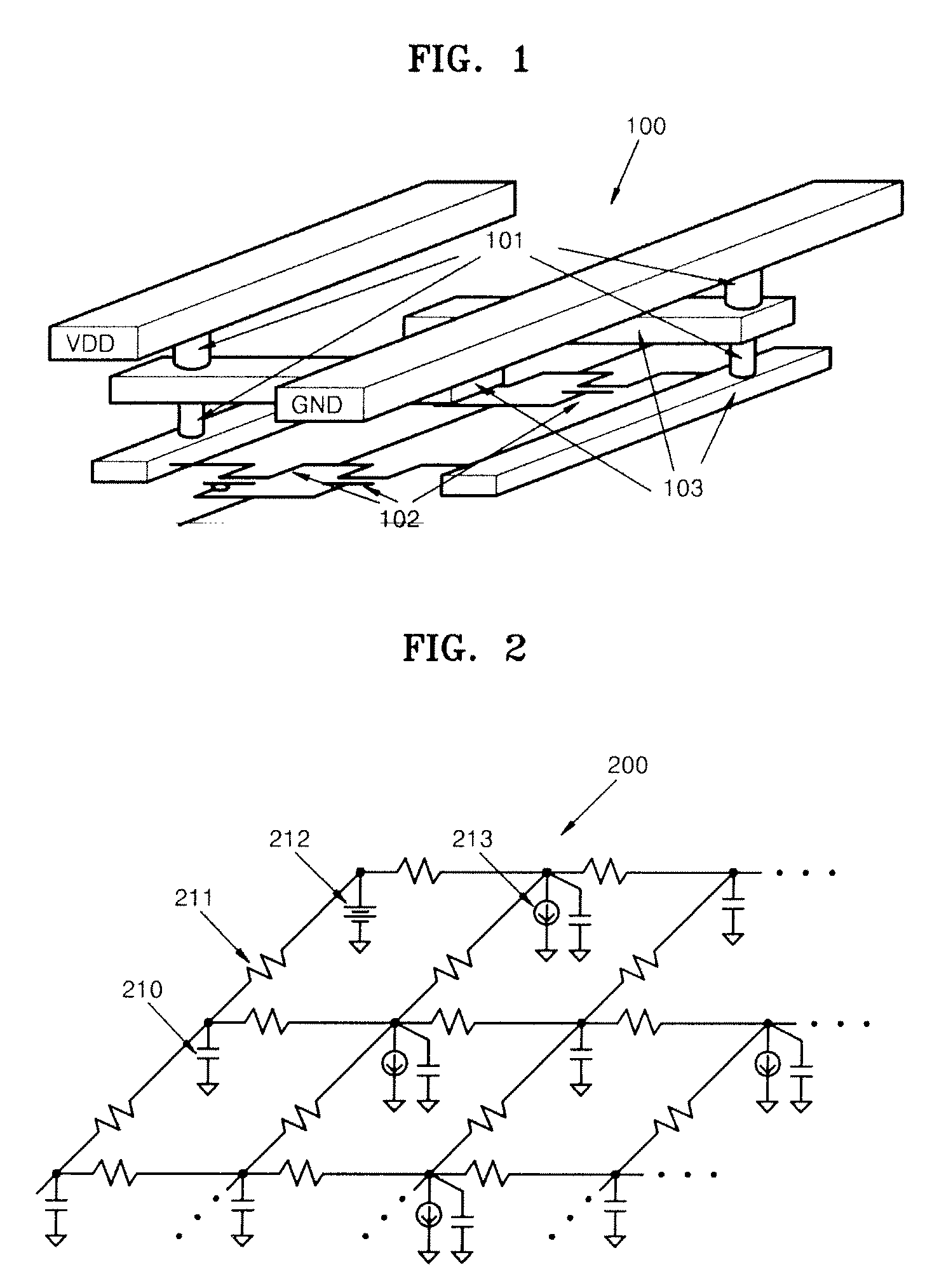
[0023]FIG. 1 is a schematic diagram illustrating a portion of a power distribution network 100 of an integrated circuit, according to an embodiment of the present invention Power distribution within a very large scale integration (VLSI) circuit is performed from the top level of a metal layer of the power distribution network 100. Referring to FIG. 1, the top level of the metal layer is connected to a package through interlayer vias 101, and finally to an active device 102. Metal wires 103 and the interlayer vias 101 are modeled as a linear, time invariant, and passive network consisting of resistive, capacitive, and rarely-inductive elements. A power network of a VLSI circuit, such as a microprocessor, can include millions of nodes and tens of millions of electrical devices. Models of power sources and drains ca...


PUM


Abstract

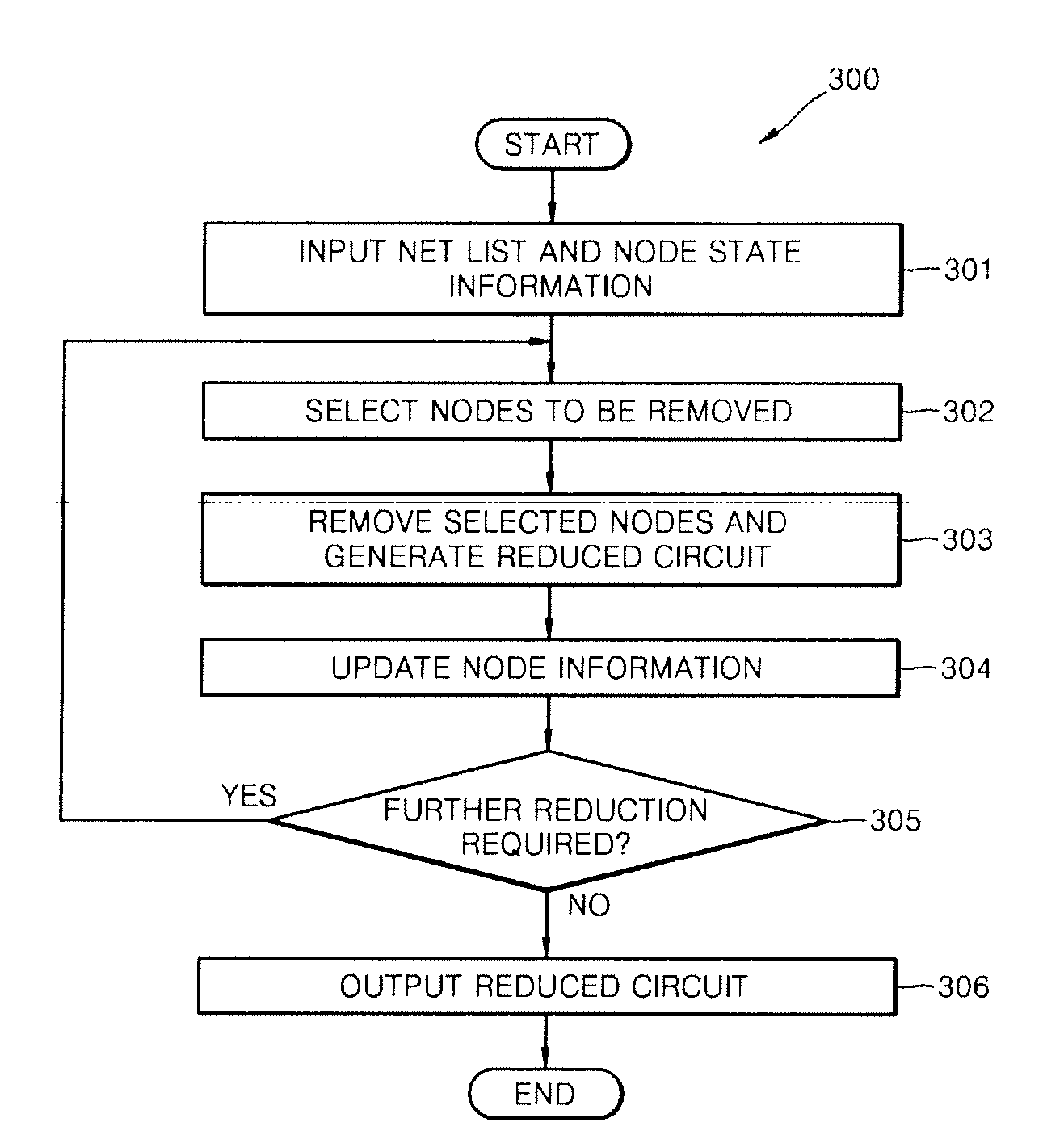
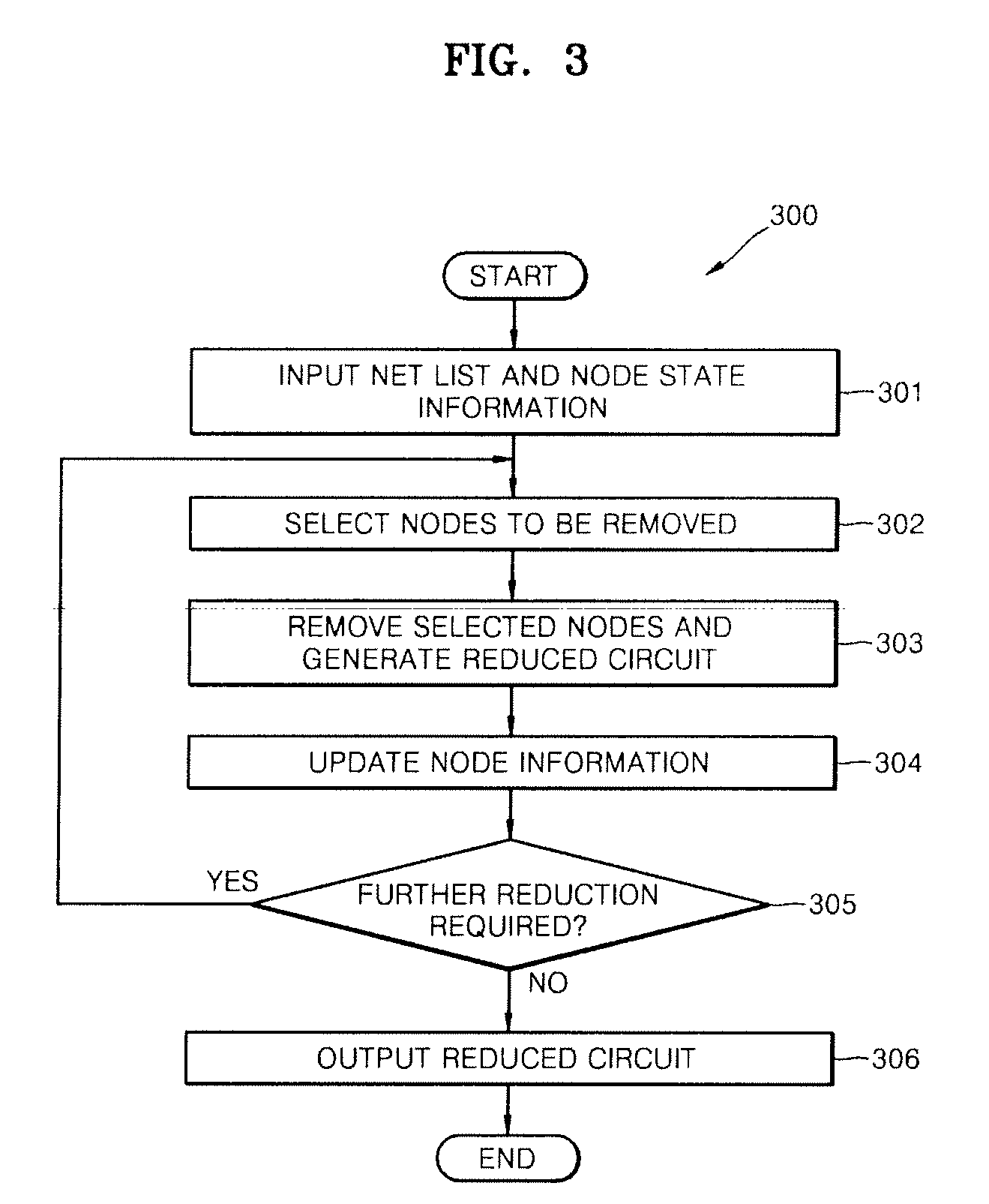
Provided are a method and apparatus for analyzing a circuit model by reducing, and a computer program product for analyzing the circuit model. The circuit model at least includes independent current source models, resistance models, and capacitance models. Also, the circuit model forms a resistance capacitance (RC) network with independent current sources. The method includes selecting a node to be removed using resistance information and comparing conductance of a capacitor for a given time step and the total conductance of the node. Further, the method includes removing the selected nodes and generating RC elements and independent current sources using adjacent nodes, which maintain the accuracy of node voltages of a circuit reduced in an accuracy order used for entrywise perturbation of the corresponding circuit equation. Moreover, an efficient method of handling the independent current sources while reducing the circuit is provided.

Description

CROSS-REFERENCE TO RELATED PATENT APPLICATION[0001]This application claims the benefit of Korean Patent Application No. 10-2007-0019929, filed on Feb. 27, 2007, in the Korean Intellectual Property Office, the disclosure of which is incorporated herein in its entirety by reference.BACKGROUND OF THE INVENTION[0002]1. Field of the Invention[0003]The present invention relates to a method and apparatus for analyzing a circuit model by reduction, and a computer program product for analyzing the circuit model, and particularly, to a method and apparatus for efficiently analyzing a circuit model which includes a large number of linear floating resistances, an RC network formed of a grounded capacitance, and a large number of independent current sources, and a computer program product for analyzing the circuit model.[0004]More particularly, the present invention relates to a method and apparatus for analyzing a circuit model by reduction, which can maintain the same level of node voltage in ...

Claims


Application Information

Patent Timeline
IPC IPC(8): G06F17/50
CPCG06F2217/78G06F17/5036G06F30/367G06F2119/06
Inventor CHE, HONG BOKIM, YOUNG HWAN
Owner POSTECH ACAD IND FOUND
Learn More