Method of Forming Organic Compound Layer, Method of Manufacturing Organic El Element and Organic El Element

a technology of organic compound and manufacturing method, which is applied in the field of forming organic compound layer, method of manufacturing organic el element and organic el element, can solve the problems of increasing cost, large surface area, and high cost of manufacturing a full color display element having a large area, and achieves high quality withou, the effect of increasing the cos

Active Publication Date: 2008-09-04
MERCK PATENT GMBH
View PDF9 Cites 43 Cited by
  • Summary
  • Abstract
  • Description
  • Claims
  • Application Information

AI Technical Summary

Benefits of technology

[0050]The present invention provides a highly productive method to form an organic compound layer for an organic EL element application having a high quality without increase of a cost, manufacturing method of an organic EL elemen...

Problems solved by technology

In any of these methods, an apparatus becomes large as well as a cost becomes high to manufacture a full color display element having a large area because a sheet form substrate is utilized as a substrate.
1) The using efficiency of an organic substance, which is utilized to form one or a plural number of emission layers comprising an organic substance is low, which is one reason to increase the cost.
2) Since it is a method to form one or a plural number of emission layers comprising an organic substance by an evaporation method, it is difficult to scale up because an evaporation room has to be made larg...

Method used


Image

  • Method of Forming Organic Compound Layer, Method of Manufacturing Organic El Element and Organic El Element
  • Method of Forming Organic Compound Layer, Method of Manufacturing Organic El Element and Organic El Element
  • Method of Forming Organic Compound Layer, Method of Manufacturing Organic El Element and Organic El Element

Examples


example 1

Preparation of Flexible Band Substrate Provided with Gas Barrier Layer and First Electrode Layer in this Order

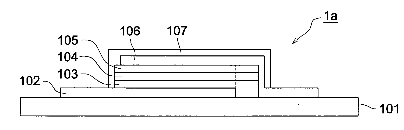
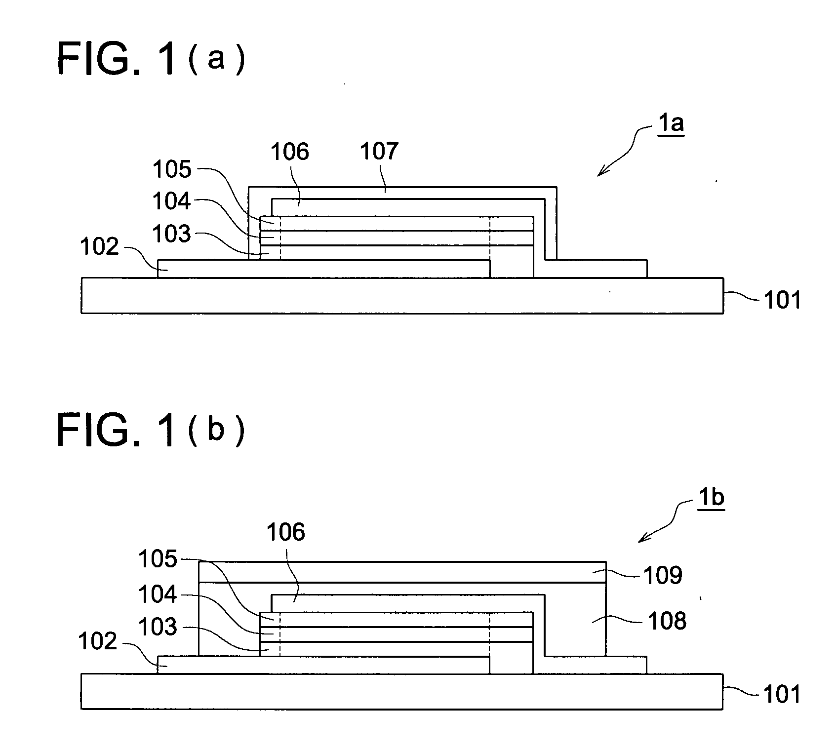
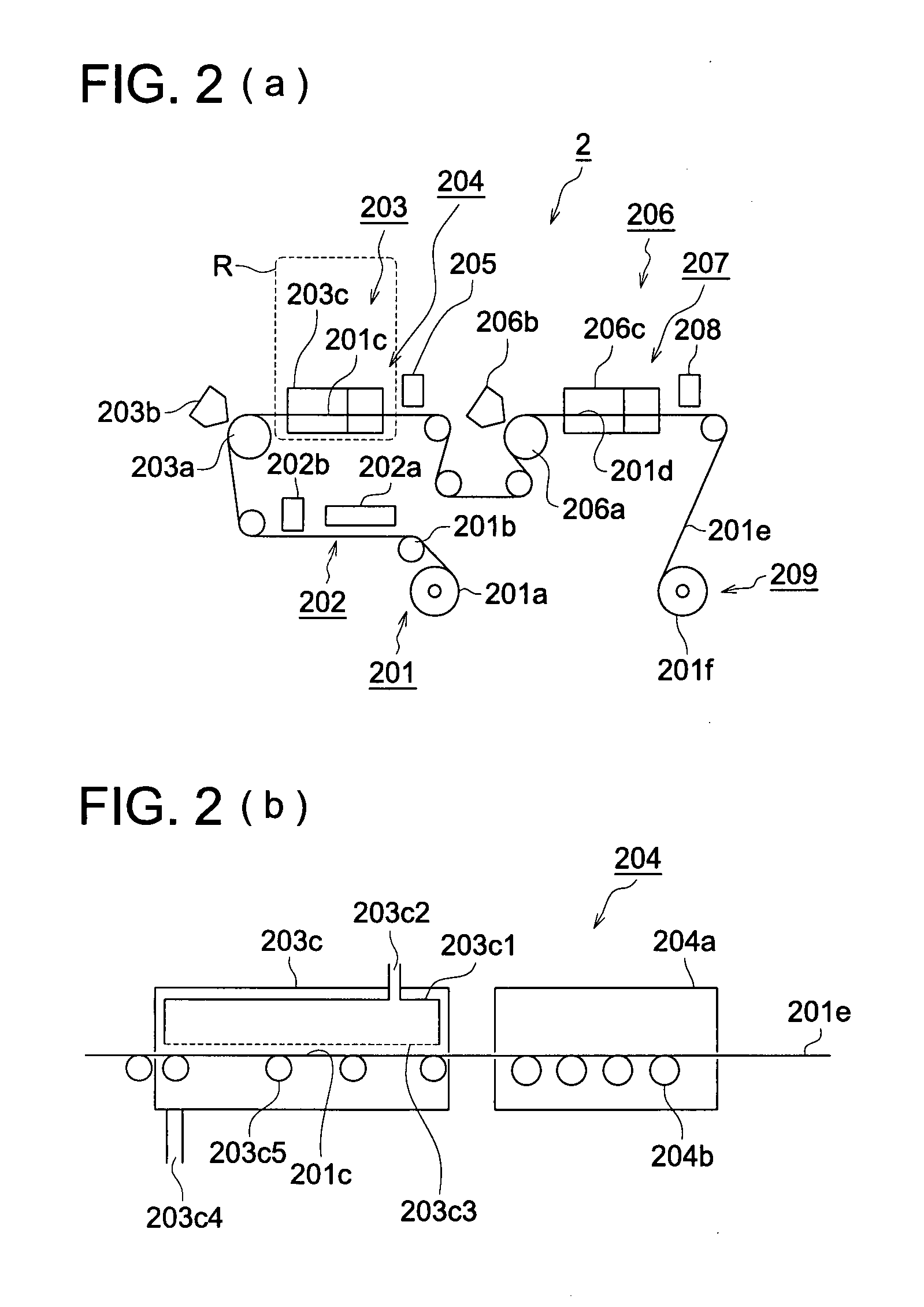
[0224]A gas barrier layer and the first electrode layer were formed by the following method on polyether sulfone having a thickness of 200 μm (film manufactured by Sumitomo Bakelite Co., Ltd., hereinafter referred to as PES), which was wound on a core to be a roll from, whereby a flexible band substrate provided with a gas barrier layer and the first electrode layer in this order was prepared.

Formation of Transparent Gas Barrier Layer

[0225]A transparent gas barrier layer having a thickness of approximately 90 nm was formed on the prepared PES by an atmospheric pressure discharge treatment method. Water vapor permeability was measured by a method based on JISk-7129B to be not more than 10−3 g / m2 / day. Oxygen permeability was measured by a method based on JISk-7126B to be not more than 10−3 g / m2 / day.

Formation of First Electrode Layer

[0226]ITO (indium tin oxide) having a thickne...

example 2

[0245]An organic compound layer was formed in a similar manner to preparation of sample No. 103 in example 1 except that a drying condition (an air ejection velocity, a variation of air ejection velocity in the coated film width direction of an organic compound layer) after an organic compound layer coating solution having been coated was changed as shown in table 2, being cooled down to room temperature, the resulting substrate was wound on a core to make a roll form, whereby sample Nos. 201-214 were prepared. Herein, an air ejection velocity was measured by hot air anemometer Model 6113, manufactured by Kanomax Co., Ltd., and a wind velocity distribution in the width direction was calculated by the following equation.

Wind velocity distribution=(maximum wind velocity−minimum wind velocity) / mean wind velocity×100

[0246]Evaluation

[0247]With respect to prepared sample Nos. 201-214, the state of a coated surface was visually evaluated and the evaluation result based on the following eva...

example 3

[0252]An organic compound layer was formed in a similar manner to preparation of sample No. 103 in example 1 except that a surface tension of an organic compound layer coating solution was changed as shown in table 3, being cooled down to room temperature, the resulting substrate was wound on a core to make a roll form, whereby sample Nos. 301-307 were prepared. Herein, a surface tension was measured by surface tension meter CBVP-A3, manufactured by Kyowa Interface Science Co., Ltd.

[0253]Evaluation

[0254]With respect to prepared sample Nos. 301-307, the state of a coated surface was visually evaluated and the evaluation result based on the following evaluation ranks is shown in table 2.

[0255]A: No unevenness and no mottle, of the coated layer surface, are observed.

[0256]B: Slight unevenness and mottle, of the coated layer surface, which is not problematic in practical use, are partly observed.

[0257]C: Unevenness and mottle, of the coated layer surface, are observed all over the surfa...


PUM

PropertyMeasurementUnit
Temperatureaaaaaaaaaa
Fractionaaaaaaaaaa

Abstract

A method of forming an organic compound layer for producing organic EL element exhibiting high quality and high productivity without increasing cost; a relevant process for producing an organic EL element. There is provided a method of forming an organic compound layer of organic EL element using production apparatus including supply section, coating•drying section and recovery section, characterized in that flexible band substrate (A) having an anode layer in roll form is fed to the supply section; the production apparatus has at least one unit coating•drying section, the unit containing coating section capable of forming coating film for formation of organic compound later under atmospheric pressure by wet applicator and drying section; and at least one organic compound layer is formed on the anode layer to obtain flexible band substrate (B), which is wound on a core to form a roll in the recovery section.

Description

FIELD OF THE INVENTION[0001]The present invention relates to a method of forming an organic compound layer of an organic EL element which is applied for such as a plane light source and a display panel, a manufacturing method of an organic EL element and an organic EL element manufactured by said method.BACKGROUND[0002]In recent years, an organic EL element utilizing an organic substance has a bright prospect of application as a low priced full color display element having a large area and a light source alley for writing, as a solid emission type, and active research and development thereof is on the way. An organic EL element is a thin film type element which is provided with the first electrode (a cathode or an anode), an organic compound layer (comprising a single layer or plural layers) containing an organic emission substance being accumulated thereon, that is a light emission layer, and the second electrode (a cathode or an anode) accumulated on said light emission layer. Whe...

Claims


Application Information

Patent Timeline
IPC IPC(8): B32B9/04H05B33/10
CPCH05B33/10
Inventor TAKASHIMA, NOBUHIKOTOBISAWA, SEIICHIMURAYAMA, MASAAKITAKASHIMA, YOUSUKE
Owner MERCK PATENT GMBH
Why Eureka
Try Eureka