Probe tips

a technology of probe tips and tips, which is applied in the direction of instruments, mechanical roughness/irregularity measurements, measurement devices, etc., can solve the problems of requiring a great deal of miniaturization, not being able to provide enough sharp or uniform tips to produce, and still requiring a great deal of optimization and characterization. , to achieve the effect of small apex radii

Inactive Publication Date: 2008-09-11
CERES DONATO +2
View PDF0 Cites 7 Cited by
  • Summary
  • Abstract
  • Description
  • Claims
  • Application Information

AI Technical Summary

Benefits of technology

[0004]In one embodiment, this invention describes a method for fabricating metal-coated AFM tips that can feature (1) very small apex radii and (2) extremely uniform coatings independent of the underlying tip shapes. Conductive probes presenting these two features can have numerous advantages compared to current probes.

Problems solved by technology

As semiconductor device features are continuously shrinking, technologies able to test new devices are requiring a great deal of miniaturization.
Ultra-sharp metallic tips can be of particular utility for memories based on conductance modification, however tip shape is extremely important for bit read / write and current coating techniques are not capable of providing sufficiently sharp or uniform tips able to produce features smaller than about 100 nm.
Emerging technologies, such as carbon nanotube-modified AFM tips, are very promising, but they still require a great deal of optimization and characterization.
Additionally, methods for the fabrication of CNT conductive probe tips have not proven easily scalable to mass production, since each tip has to be individually modified and characterized.

Method used


Image

  • Probe tips
  • Probe tips
  • Probe tips

Examples


Embodiment Construction

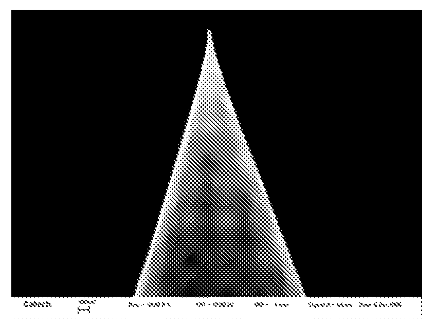
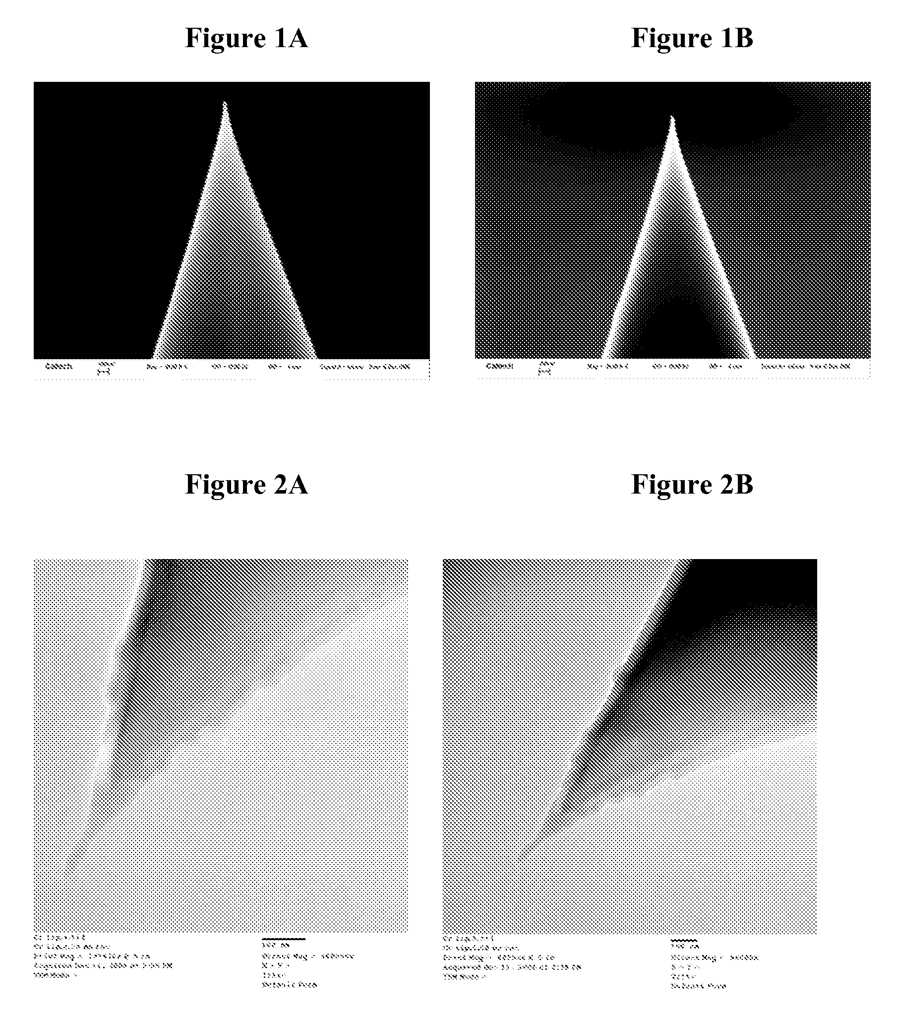
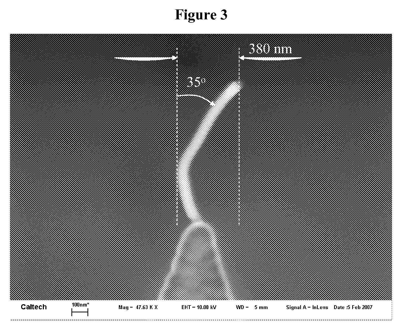
[0013]The method described herein can allow the manufacture of ultra-sharp conductive AFM tips, regardless of the quality of the underling tip shape. Typically this is achieved by using a regular silicon tip, although the tip material is not a specific requirement for the invention. In alternative embodiments, the tip can be made of silicon nitrate. In preferred embodiments of the present invention, an AFM tip is placed in a sputter coater equipped with a planetary rotating stage. In alternative embodiments, metal evaporation based on resistive heating or an electron beam can be used for the purpose of the invention. Referring to FIGS. 1 and 2, a planetary rotating stage will allow the tip to be coated uniformly and enable the metal coating to grow regularly around the tip apex to form the ultra sharp metallic tip.

[0014]The deposited metal can be of different nature. Referring to FIGS. 2A and 2B, a single layer of 10 to 20 nm thickness of a metal, such as chromium can be used to pro...


PUM

PropertyMeasurementUnit
thicknessaaaaaaaaaa
sizeaaaaaaaaaa
thicknessaaaaaaaaaa

Abstract

Probe tips comprising tips and coatings are described. The tips and coatings may be selected to provide various probe-tip features, including, but not limited to, high reproducibility, high reliability, low cost, ultra-sharpness, high conductivity and/or simultaneous critical dimension imaging and sidewall roughness analysis.

Description

[0001]This application claims priority to U.S. Provisional Patent Application No. 60 / 894,141, filed Mar. 9, 2007 and entitled “METHOD FOR FABRICATING CURVED CARBON NANOTUBES FOR CRITICAL DIMENSION IMAGING” and U.S. Provisional Patent Application No. 60 / 894,133, filed Mar. 9, 2007 and entitled “METHOD FOR FABRICATING ULTRA SHARP AND UNIFORM TIPS FOR PROXIMAL PROBE MICROSCOPES,” which are hereby incorporated herein by reference.BACKGROUND OF THE INVENTION[0002]As semiconductor device features are continuously shrinking, technologies able to test new devices are requiring a great deal of miniaturization. Atomic force microscopy (AFM) is very useful for investigating small topographical features of the devices, but with a conductive probe it is possible to investigate also local electrical properties of the device. Metal-coated AFM tips are very useful for this purpose. In addition to probe new generation devices, conductive probes are also used for high-density data storage. The probe ...

Claims


Application Information

Patent Timeline
Patent Type & Authority Applications(United States)
IPC IPC(8): G01B5/28G01D21/00
CPCB82Y15/00G01Q70/12G01Q60/40B82Y35/00
Inventor CERES, DONATONARUI, YOSHIECOLLIER, CHARLES PATRICK
Owner CERES DONATO
Why Eureka
Try Eureka