Micro/Nano-Pattern Film Contact Transfer Process

a technology of nano-patterns and contact layers, applied in the field of micro-/nano-pattern film contact transfer process, can solve the problems of easy distortion or damage of patterns during the removal process of residual layers, time-consuming rise and decrease of temperature, and prolong the life of molds , the effect of easy mold manufacturing process

Inactive Publication Date: 2008-09-11
NAT CHENG KUNG UNIV
View PDF4 Cites 13 Cited by
  • Summary
  • Abstract
  • Description
  • Claims
  • Application Information

AI Technical Summary

Benefits of technology

[0008]Another aspect of the present invention is to provide a micro / nano-pattern film contact transfer process, in which a transferring process can be performed by a very small pressure, so that the life of the mold is prolonged.
[0009]Still another aspect of the present invention is to provide a micro / nano-pattern film contact transfer process, in which a non-flexible mold can be used to perform the transferring of a micro / nano-pattern film, so that the issue of being difficult to control the size of the feature pattern of the flexible material can be overcome.
[0010]Further another aspect of the present invention is to provide a micro / nano-pattern film contact transfer process, in which a surface modification step is performed on a pattern surface of a mold to make the pattern surface have a mold-releasing effect, so that the ability of successfully transferring the transfer layer contacting with the substrate to the substrate after contacting, heating and pressing is enhanced, thereby successfully forming the desired transferring pattern.
[0011]Yet another aspect of the present invention is to provide a micro / nano-pattern film contact transfer process, in which a mold can be composed of a silicon material, so that the manufacturing process of the mold is easy, the mold is cheap, and the selectivity of the mold material is various. Accordingly, various tiny patterns can be formed depending on the selection of the materials and the lattice characteristics of the materials, so that the desired structure can be easily formed on the mold, thereby increasing the variety of the nano-imprinting technique.
[0013]According to the aforementioned aspects, the present invention provides a micro / nano-pattern film contact transfer process, comprising: providing a mold including a first surface and a second surface on opposite sides, and an imprinting pattern is set in the first surface of the mold; forming a release layer on the first surface of the mold; forming a transfer material layer on a surface of the release layer; providing a substrate including a first surface and a second surface on opposite sides; putting the mold together with the substrate to make the first surface of the mold be opposite to the first surface of the substrate; applying a pressure to make the first surface of the substrate closely contact with the transfer material layer on the first surface of the substrate, wherein the pressure is a uniform pressure or a concentrated pressure, when the step of applying the pressure is performed by applying the concentrated pressure, the pressure is continuously applied through a transparent cylinder, and the transparent cylinder can provide the heating source with a focus effect; providing a heating source to heat the transfer material layer, so as to produce an adhesion effect between a portion of the transfer material layer contacting with the first surface of the substrate and the first surface of the substrate; and removing the mold, wherein the contacting portion of the transfer material layer is transferred onto the first surface of the substrate.

Problems solved by technology

However, the hot embossing technique and a flexible nano-transferring technique respectively have some disadvantages.
With regard to the hot embossing technique, a polymer material has to be used as a mask layer after transferring, and the residual layer after imprinting needs to be removed, so that the pattern is easily distorted or damaged during the removal process of the residual layer.
In addition, it needs to cost dozens of minutes to heat the polymer material on the substrate from the room temperature to the temperature above the glass transition temperature and then to cool down the temperature of the polymer material to the room temperature, so that the rise and the decrease of the temperature both are time-consuming, which is very unfavorable to mass production.
In addition, the polymer material, such as PDMS, is a flexible material, so that it is difficult to control the size of the feature pattern.

Method used


Image

  • Micro/Nano-Pattern Film Contact Transfer Process
  • Micro/Nano-Pattern Film Contact Transfer Process
  • Micro/Nano-Pattern Film Contact Transfer Process

Examples


Embodiment Construction

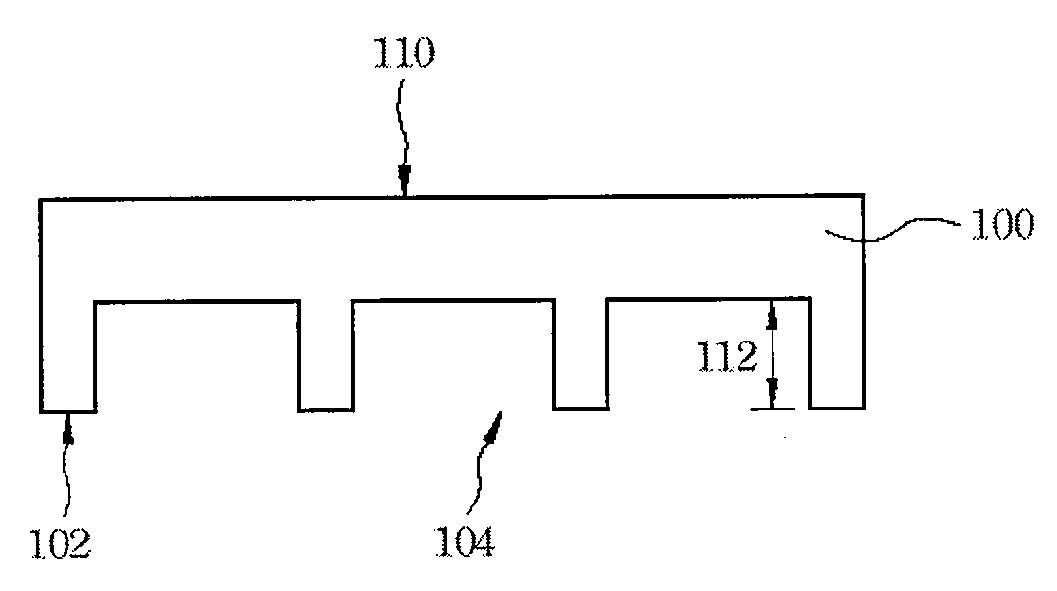
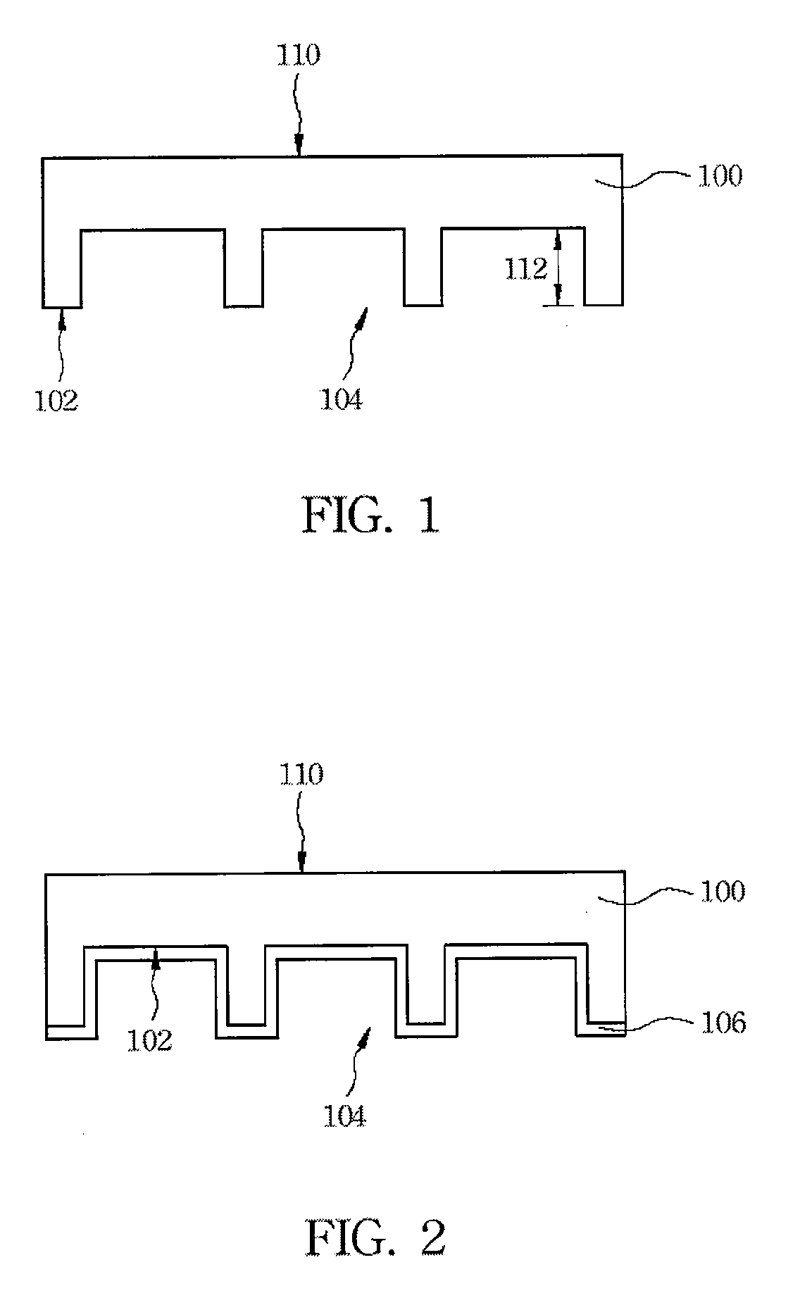
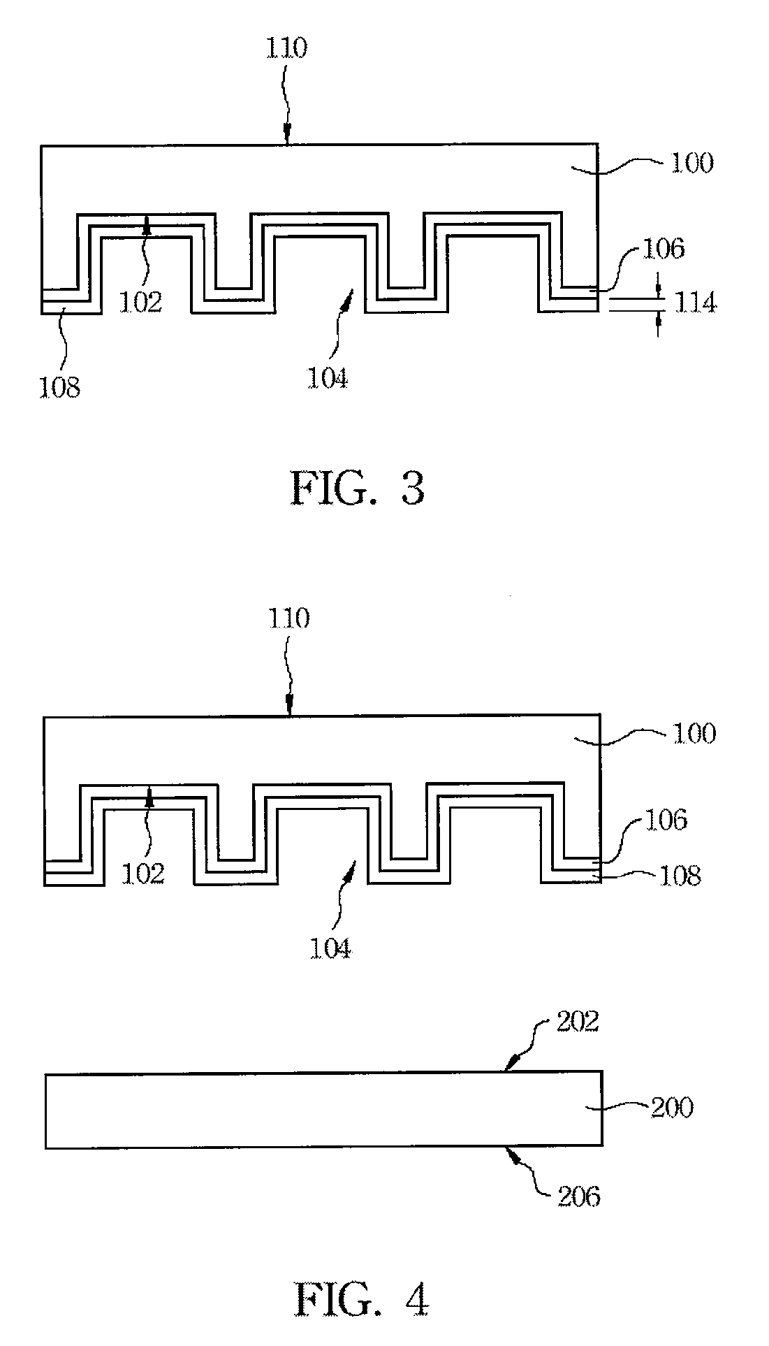
[0018]The present invention discloses a micro / nano-pattern film contact transfer process, which can directly transfer a transfer material onto a substrate, so that it is unnecessary to use a polymer material to form an etching mask in the sequential etching process, a pattern required by a nano-device can be directly defined and arrayed on the substrate, the transfer material is more various, and the problem of being difficult to control the size of a feature pattern of a flexible material can be solved. Accordingly, the transferring technique can achieve a large-area objective and advantages including low cost, rapid and mass production. In order to make the illustration of the present invention more explicit, the following description is stated with reference to FIGS. 1 through 11B.

[0019]FIGS. 1 through 10 are schematic flow diagrams showing micro / nano-pattern film contact transfer processes in accordance with preferred embodiments of the present invention. In an exemplary embodim...


PUM

PropertyMeasurementUnit
light wavelengthaaaaaaaaaa
wavelengthaaaaaaaaaa

Abstract

A micro / nano-pattern film contact transfer process is described, comprising: providing a mold, wherein an imprinting pattern is set in a first surface of the mold; forming a release layer on the first surface of the mold and a transfer material layer on the release layer; providing a substrate; placing the mold on a first surface of the substrate, wherein the first surface of the mold is opposite to the first surface of the substrate; applying a pre-pressed force on the substrate from a second surface opposite to the first surface of the substrate; providing a heating source to heat the transfer material layer to produce an adhesion effect between a portion of the transfer material layer contacting with the first surface of the substrate and the substrate; and removing the mold, wherein the contacting portion of the transfer material layer is transferred onto the first surface of the substrate.

Description

RELATED APPLICATIONS[0001]This application claims priority to Taiwan Application Serial Number 95126597, filed Jul. 20, 2006, which is herein incorporated by reference.FIELD OF THE INVENTION[0002]The present invention relates to an imprinting process, and more particularly, to a micro / nano-pattern film contact transfer process.BACKGROUND OF THE INVENTION[0003]Currently, the common imprinting techniques mainly include a hot embossing technique and a flexible nano-transferring technique. In the hot embossing technique, a substrate or a material coated on the substrate is heated by electrical resistance heating, and then a surface including an imprinting pattern of a mold is pressed into the substrate or the material on the substrate to make the imprinting pattern transfer into the substrate or the material on the substrate. In the flexible nano-transferring technique, a mold may be composed of a flexible polymer material, such as PDMS, next a self-assembly monomer is coated on a surfa...

Claims


Application Information

Patent Timeline
Patent Type & Authority Applications(United States)
IPC IPC(8): B29C59/16
CPCB29C35/0888B29C37/0067B29C59/022B29C59/16G03F7/0002B29C2035/0838B29C2059/023B82Y10/00B82Y40/00B29C2035/0822
Inventor LEE, YUNG-CHUNLIU, CHUAN-PUHSIAO, FEI-BINCHEN, CHUN-HUNGCHIU, CHENG-YU
Owner NAT CHENG KUNG UNIV
Why Eureka
Try Eureka