Programmable logic integrated circuit for digital algorithmic functions

Inactive Publication Date: 2008-09-11
QUADRIC
View PDF3 Cites 46 Cited by
  • Summary
  • Abstract
  • Description
  • Claims
  • Application Information

AI Technical Summary

Benefits of technology

[0018]In accordance with the invention, per-cycle programmable functionality and interconnect are combined into instructions that encompass general functionality. Using this general functionality, computing power can be focused after implementation on design bottle

Problems solved by technology

Although this is similar to the reprogramming capability of an FPGA, the processor, relying on the storage of inactive instructions, achieves hardware reuse in real time with a very limited instruction set.
Because it is architected to address broad functionality, a processor has limitations in its performance, especially when computing functions which have strict throughput constraints.
However, these customizations make the processor less general, reducing its applicability to certain other functions.
Current integrated circuit processors do not provide a customization path to address general sequential and concurrent computational bottlenecks of control and data after implementation of the processor, i.e., there is no mechanism to incorporate the hardware capability of ASIC or FPGA designs.
Because of the complexity of the design elements, both technologies require a very detailed analysis of timing delays associated with the computational and interconnect elements to verify the correct functionality of the design.
ASIC technology has high performance and low recurring cost, but can cost tens of millions of dollars to design and produce at 180 nm and below.
The technology is hard-wired, meaning that it cannot be changed once it is manufactured.
Design

Method used


Image

  • Programmable logic integrated circuit for digital algorithmic functions
  • Programmable logic integrated circuit for digital algorithmic functions
  • Programmable logic integrated circuit for digital algorithmic functions

Examples


first embodiment

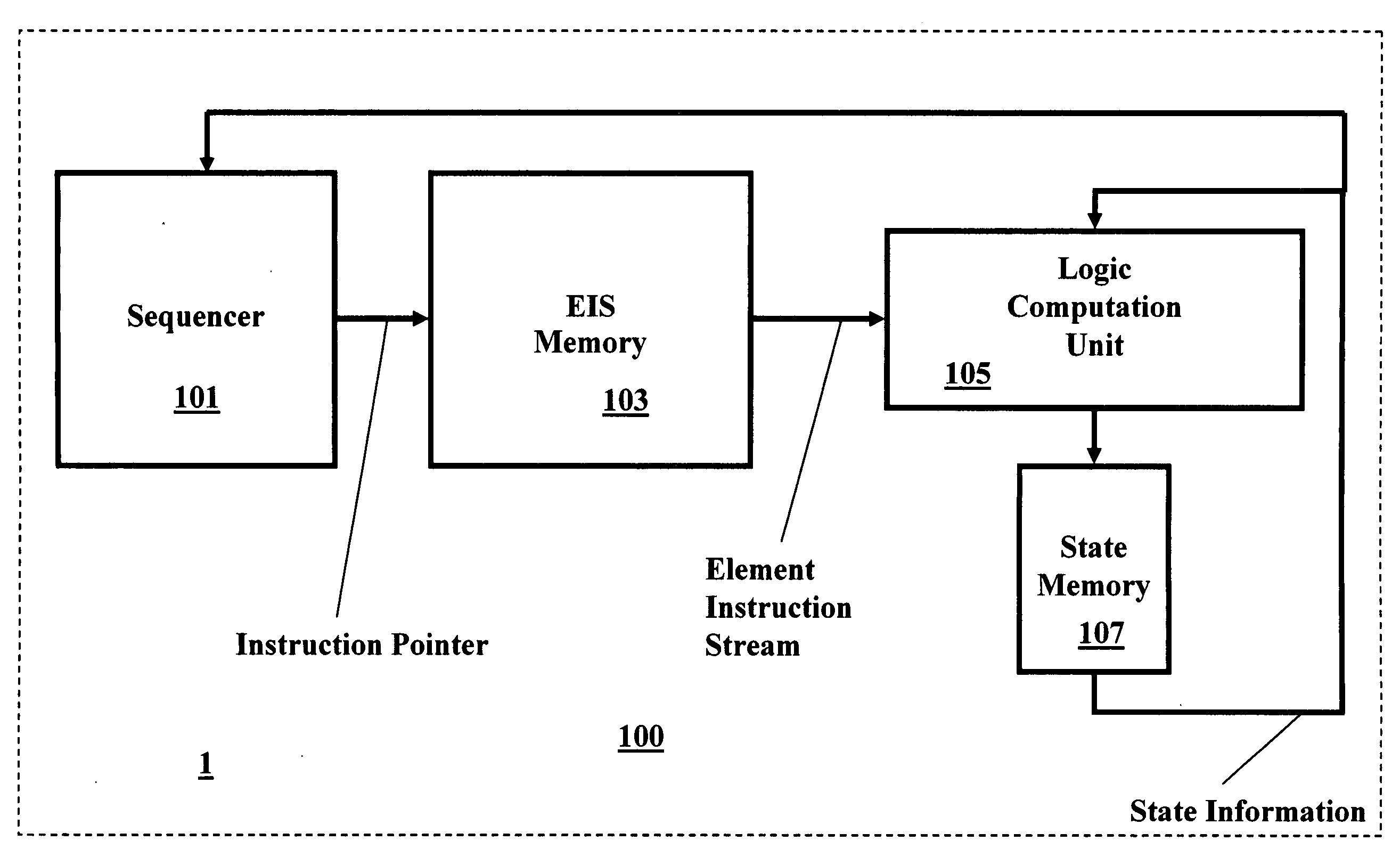
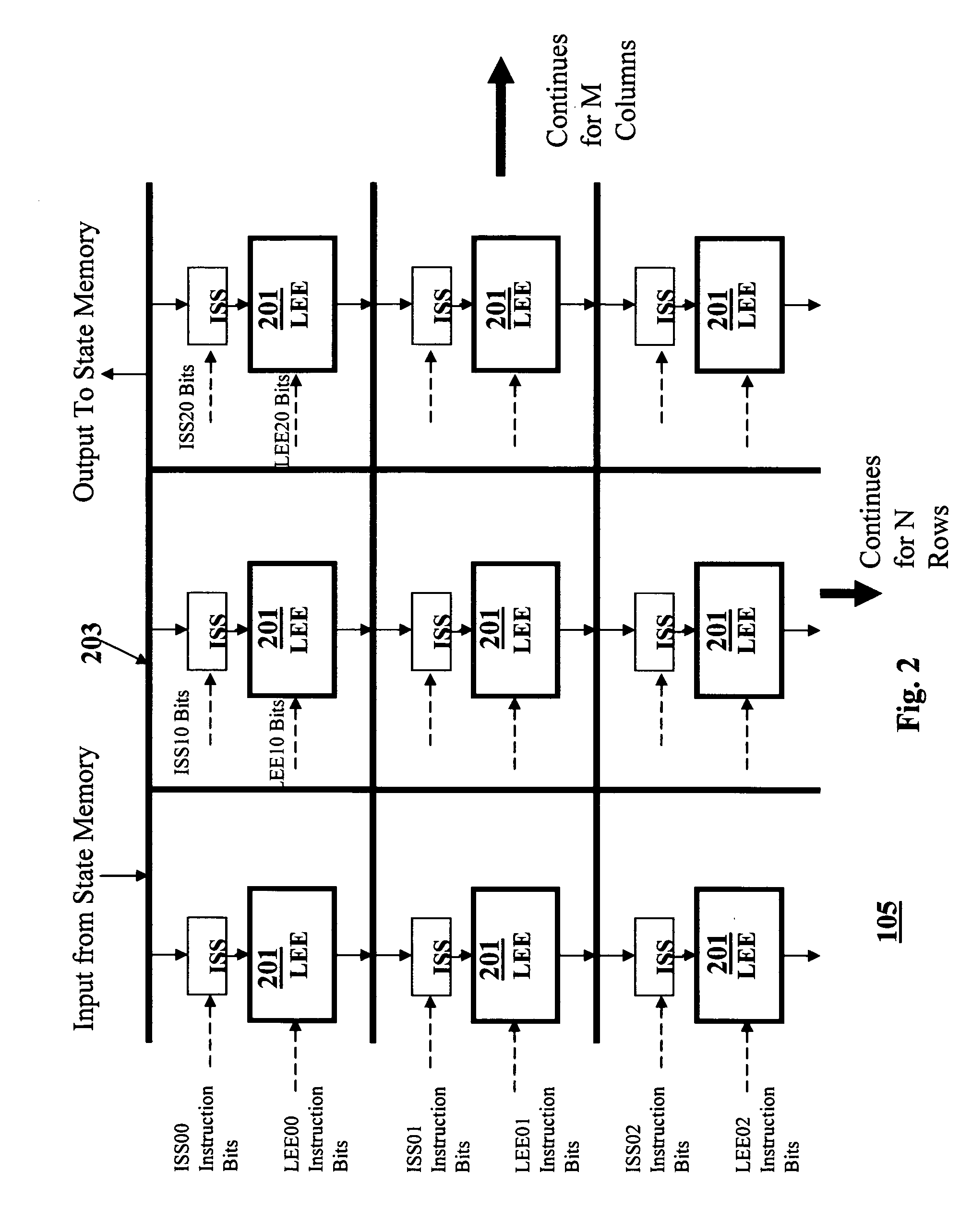
[0058]a logic computation unit LCU 105 is shown in FIG. 2. Logic computation unit LCU 105 comprises an array of a plurality of logic execution elements LEEs 201 arranged as a matrix of M columns and N rows. Each logic execution element LEE 201 performs the basic, fine-grained computation of logic functions, the aggregate of which make up an entire digital algorithm to be computed by the logic computation unit LCU 105. Logic execution elements LEEs 201 are connected by means of an interconnect matrix 203, that provides routing of signals from logic execution elements LEE 201 outputs to logic execution elements LEE 201 inputs. Each logic execution elements LEEs 201 receives inputs from interconnect matrix 203 through the use of an interconnect selection circuit ISS. Interconnect matrix 203 also receives inputs from state memory 107. State memory 107 receives and stores inputs from interconnect matrix 203.

[0059]Each logic execution element LEE 201 and input source select ISS take a por...

second embodiment

[0064]input source select ISS shown in FIG. 4B is an analog crosspoint switch 403. A number of bits from interconnect matrix 203 is input to crosspoint switch 403. The instruction bits select which input bits get connected to which outputs. This performs the exact same function as multiplexer 401 but is a different physical mechanism to achieve the same function.

[0065]There are many ways to connect interconnect matrix 203 to the individual input source select ISS units. In some embodiments, the connection might be universal, that is, all bits of the interconnect matrix 203 are connected to each input source select ISS. In other embodiments, only certain bits of the matrix 203 are connected to each input source select ISS. In one such embodiment all input source selects ISS within a X by Y portion of the logic computation unit LCU array 105 are interconnected. Thus every logic execution element LEE 201 has inputs from all of its immediate neighbors. In another embodiment, each row of...


PUM


Abstract

A programmable integrated circuit for calculating a digital algorithm is disclosed. The integrated circuit is programmable to operate on input data in accordance with one or more predetermined digital algorithms.

Description

RELATED APPLICATIONS[0001]This application claims priority from and the benefit of Provisional Application for Patent Ser. No. 60 / 905,947 filed Mar. 9, 2007.FIELD OF THE INVENTION[0002]The invention pertains to software programmable system architecture, in general, and to software programmable integrated circuit system architecture that can be programmed to provide algorithmic digital functions, in particular.BACKGROUND OF THE INVENTION[0003]Algorithm based digital functions in electronic systems are typically implemented in one of two ways: with an integrated circuit micro-processor or a custom integrated circuit including application specific integrated circuits ASICs and field programmable gate arrays FPGAs. Each has its advantages and disadvantages and the selection of which to use is an important consideration. The electronic system designer must balance many factors including performance, power, availability of talent, time to market, design cost, and production cost.[0004]Com...

Claims


Application Information

Patent Timeline
IPC IPC(8): H03K19/173
CPCH03K19/17776H03K19/17736H03K19/17758
Inventor ARRIENS, DEAN J.SHORT, PAUL
Owner QUADRIC
Why Eureka
Try Eureka