Semiconductor device with ferro-electric capacitor

Inactive Publication Date: 2008-09-18
FUJITSU SEMICON LTD
View PDF31 Cites 16 Cited by
  • Summary
  • Abstract
  • Description
  • Claims
  • Application Information

AI Technical Summary

Benefits of technology

[0017]It is an aspect of the embodiments discussed herein to provide a semiconductor device including: a semiconductor substrate; a semiconductor element formed in the semiconductor substrate; an insulating film covering the semiconductor element and formed above the semiconductor substrate; a lower insulating hydrogen diffusion preventive film having a hydrogen/moisture shielding function and formed above the insulating film; a conductive adhesion enhancing film formed above the lower insulating hydrogen diffusion preventive film; and a f

Problems solved by technology

As moisture reaches a capacitor particularly a ferro-electric capacitor, the characteristics of a dielectric film particularly a ferro-electric film are deteriorated.
If the ferro-electric film is reduced

Method used


Image

  • Semiconductor device with ferro-electric capacitor
  • Semiconductor device with ferro-electric capacitor
  • Semiconductor device with ferro-electric capacitor

Examples


first embodiment

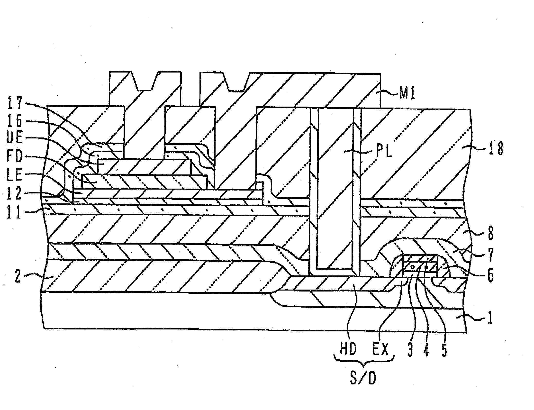
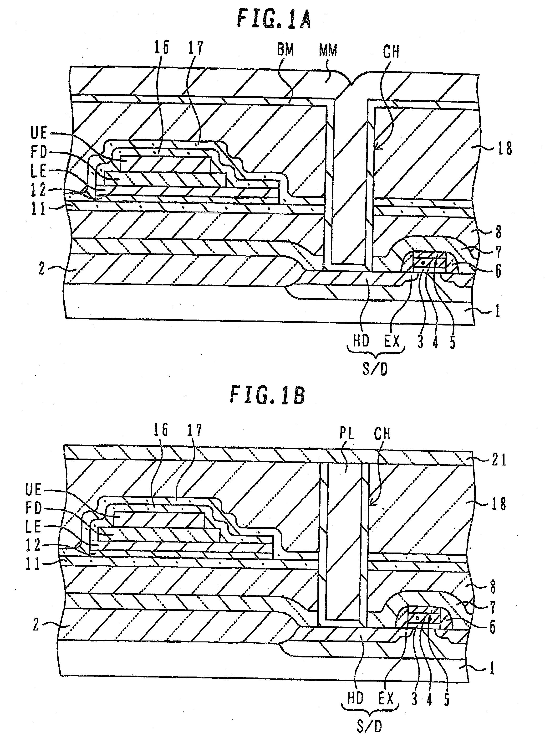
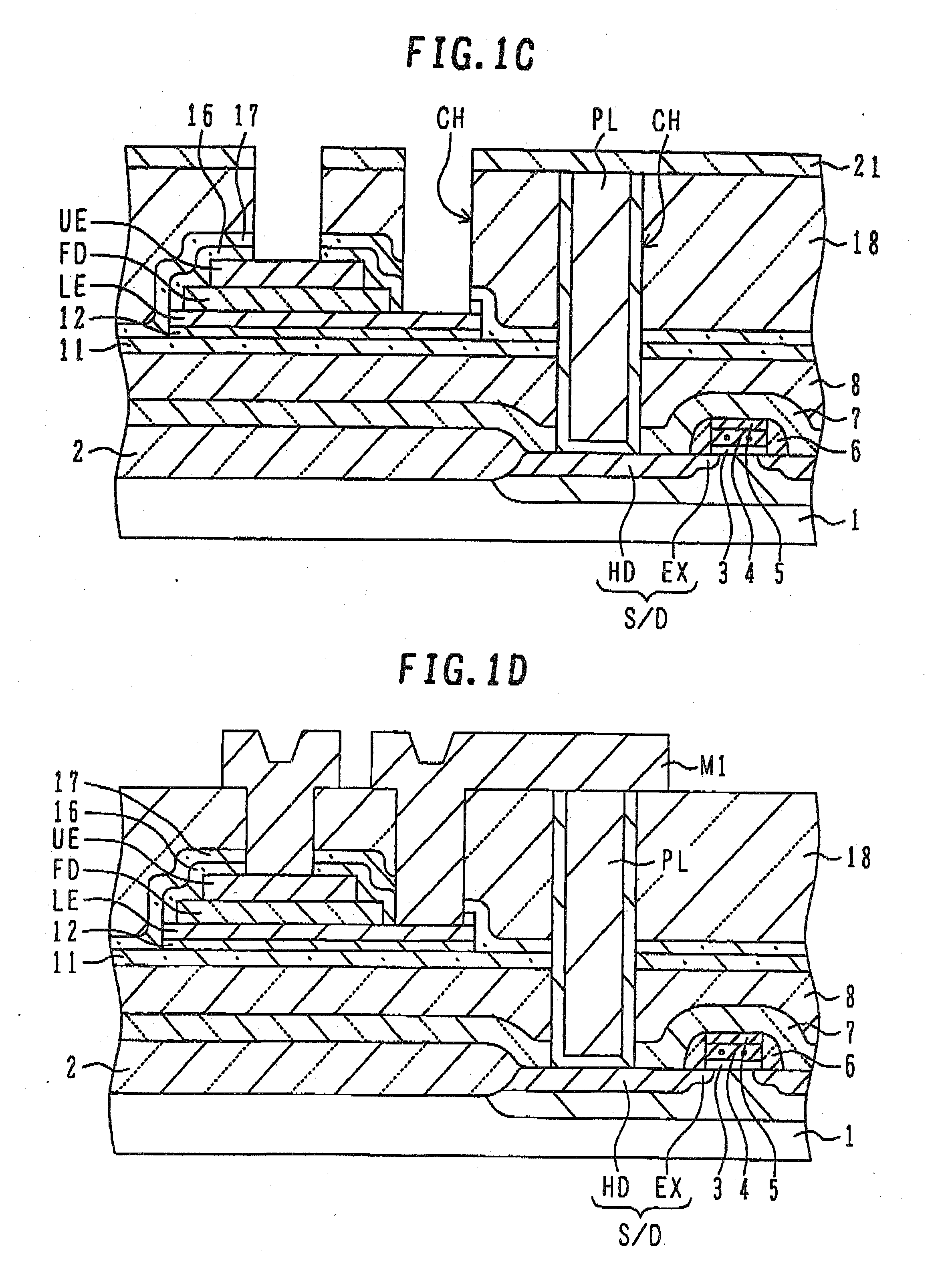
[0049]FIGS. 1A to 1D illustrate a method for manufacturing the semiconductor device of the present invention based on the above-described experiment results and show a manufactured semiconductor device.

[0050]As shown in FIG. 1A, in the surface layer of a semiconductor substrate 1 such as a silicon substrate, an isolation region defining active regions is formed, for example, by local oxidation of silicon (LOCOS). A p-type well is formed in the region where an n-channel transistor is to be formed, and an n-type well is formed in the region where a p-type transistor is to be formed. Description will be made hereinafter on forming an n-channel transistor by way of example. For the p-channel transistor, conductivity types are reversed.

[0051]The surfaces of active regions are thermally oxidized to form a gate oxide film 3 having a thickness of, e.g., 10 nm. A polysilicon film 4 and a silicide layer 5 of WSi2 are formed on the gate oxide film 3 and patterned to a gate electrode structure....

second embodiment

[0074]Description has been made on forming a planar type ferro-electric capacitor on an insulating film. A stack type is also possible, wherein a ferro-electric capacitor is formed on a conductive plug. In the following, with reference to FIGS. 6A to 6F, description will be made on the second embodiment in which a stack type ferro-electric capacitor is formed.

[0075]As shown in FIG. 6A, an isolation region 2 is formed in the surface layer of a semiconductor substrate 1 such as a silicon substrate by shallow trench isolation (STI) or the like. Ions are implanted to from a p-type well PW and an n-type well NW.

[0076]MOS transistor structures are formed by processes similar to those of the first embodiment. Namely, a gate oxide film 3 is formed by thermally oxidizing the active region surfaces, and a polysilicon film 4 and a silicide film 5 are formed and patterned to form gate electrodes. An n-type gate electrode is formed above the p-type well, and a p-type gate electrode is formed abo...


PUM


Abstract

A semiconductor device has a ferro-electric capacitor with small leak current and less process deterioration even upon miniaturization. The semiconductor device includes: a semiconductor element formed in a semiconductor substrate; lamination of an interlayer insulating film and a lower insulating shielding film having a hydrogen/moisture shielding function, the lamination being formed covering the semiconductor element; a conductive adhesion enhancing film formed above the lower insulating shielding film; and a ferro-electric capacitor including a lower electrode formed above the conductive adhesion enhancing film, a ferro-electric film formed on the lower electrode and being disposed within the lower electrode as viewed in plan, and an upper electrode formed on the ferro-electric film and being disposed within the ferro-electric film as viewed in plan, wherein the conductive adhesion enhancing film has a function of improving adhesion of the lower electrode and reducing leak current of the ferro-electric capacitor.

Description

[0001]This application is a continuation application of International Patent Application PCT / JP2005 / 21854, filed on Nov. 29, 2005, designating US as one of the designation countries, the entire contents of which are incorporated herein by reference.TECHNICAL FIELD[0002]The embodiments discussed herein are directed to a semiconductor device and a manufacture method thereof. The embodiments may relate to a semiconductor device having a ferro-electric capacitor and a manufacture method thereof.BACKGROUND ART[0003]With the recent advancement of digital technologies, there is a strong tendency toward high speed processing or storage of high capacity data, and a demand for high integration and high performance of semiconductor devices used in electronic apparatus. In order to realize high integration of a semiconductor device, as a capacitor dielectric film of a capacitor which forms a storage element, a high dielectric constant material film or a ferro-electric material film is being use...

Claims


Application Information

Patent Timeline
IPC IPC(8): H01L29/92H01L21/02
CPCH01L27/11507H01L21/02107H01L28/65H01L28/57H10B53/30H01L27/105H10B99/00H10B12/00
Inventor WANG, WENSHENGNAKAMURA, KO
Owner FUJITSU SEMICON LTD
Why Eureka
Try Eureka