Adhesive film for stacking semiconductor chips

Active Publication Date: 2008-09-18
TORAY ADVANCED MATERIALS KOREA
View PDF11 Cites 26 Cited by
  • Summary
  • Abstract
  • Description
  • Claims
  • Application Information

AI Technical Summary

Benefits of technology

[0011]The invention was devised to address the prior art technical problem as described above. It is an object of the invention to provide an adhesive film for stacking semiconductor chips in layers, with which it is not required to use separate spacers and a process of stacking the spacers in stacking the chips o

Problems solved by technology

However, for stacking the spacer, a separate process and cost is accordingly required.
As a result, delamination may occur to lower reliability of semiconductors.
However, the rubber binder resin is not well compatible with the epoxy resin composition, so that micro phase separation occurs, leading to thermal degradation of the rubber binder in the chip stacking process subject to a repeated stacking process at high temperature and thereby to lower adhesiveness, which is not desired.
If the stacked area is made different in the upper chip layer and the lower chip laye

Method used


Image

  • Adhesive film for stacking semiconductor chips
  • Adhesive film for stacking semiconductor chips
  • Adhesive film for stacking semiconductor chips

Examples


embodiment

Sample 1: Producing a First and a Third Adhesive Layer of Epoxy Resin

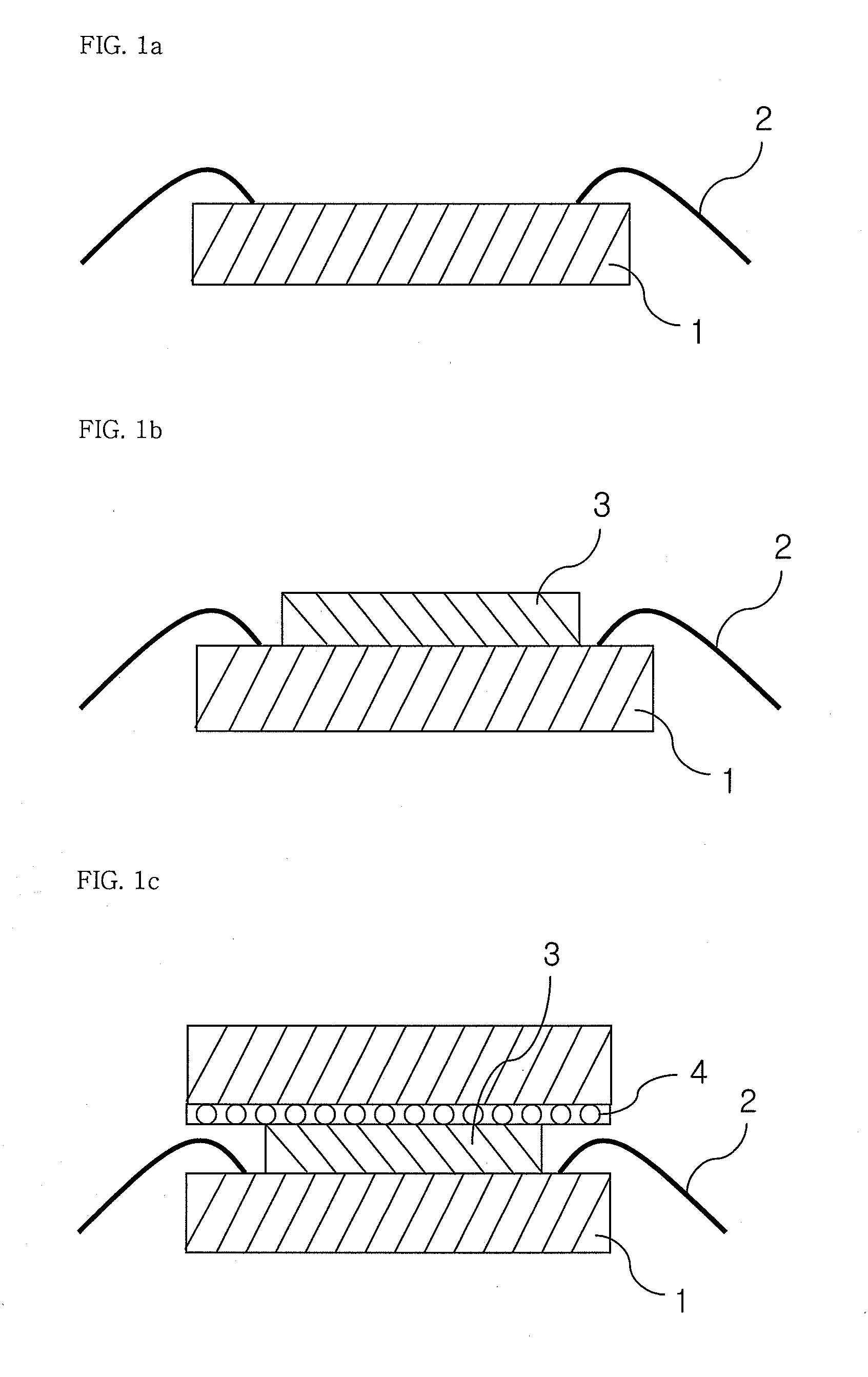
[0055]First, agitated was a mixture of 100 parts by weight of the cresol novolac epoxy resin (YDCN 8P, commercially available from Toto Kasei Co.), 50 parts by weight of the phenol novolac resin (KPH2000, commercially available from Kolon Chemical Co.), 0.02 parts by weight of 1-cyano ethyl-2-phenyl imidasol(CURE SOL 2PZ-CN, commercially available from Shikoku Kasei Co.) in a solvent of methyl ethyl ketone for 3 hours. Subsequently, 50 parts by weight of the phenoxy resin (YP50, commercially available from Toto Kasei Co.) was added to the agitated mixture, the mixture being then agitated for 6 hours again. The resulting agitated mixture was applied on a substrate of release-treated polyterephthalate film 38 μm thick. The coated film was then dried at 90° C. for 3 minutes to produce a first adhesive layer at B stage which was 40 μm thick and to produce a third adhesive layer at B stage which was 10 μm thick.

Sample 2...


PUM

PropertyMeasurementUnit
Temperatureaaaaaaaaaa
Percent by massaaaaaaaaaa

Abstract

The invention concerns an adhesive film for stacking chips which enables chips to be stacked in layers without using a separate spacer usually provided to keep a given distance between wires of an upper chip and a lower chip to have the same area. The adhesive film of the invention has an intermediate adhesive layer of thermoplastic phenoxy resin on both side of which a thermosetting adhesive layer of epoxy resin is placed, respectively, to make a three-layer structure, the thermoplastic phenoxy resin comprising UV curable small molecule compounds. The adhesive film of the invention is a multi-layered adhesive film produced by a method of comprising the steps of achieving compatibility on an interface between the thermosetting epoxy resin and thermoplastic phenoxy resin and then directly forming a phenoxy film of a high elastic modulus through UV curing in an adhesive film. With such a configuration, the adhesive film for stacking semiconductor chips according to the invention enables the semiconductor silicone chips to be stacked in 3 or more layers without using a separate spacer between chips in order to keep a wire distance between upper and lower chips in stacking the chips. With the configuration, it is advantageous that reliability of semiconductors is not lowered because adhesiveness is kept despite of a repeated process of stacking chips subject to high temperature.

Description

BACKGROUND OF THE INVENTION[0001]1. Technical field[0002]The invention relates to an adhesive film for stacking semiconductor chips, and more particularly to an adhesive film for stacking semiconductor chips that enables at least 3 layers of chips having the same area to be stacked without using any separate spacers that are sandwiched between upper and lower chips in order to keep a wire spacing between the upper and lower chips in stacking semiconductor silicone chips, and that can retain adhesiveness in a repeated stacking process subject to high temperature thus to ensure reliability of semiconductors.[0003]2. Description of the Prior Art[0004]In general, in order to enhance integration of semiconductors, a method is widely used, of stacking several layers of silicone chips by efficiently using spacers in a semiconductor package. In order to efficiently employ this stacking method, wafer backside lamination (WBL) is employed in which an adhesive film is first stacked on one side...

Claims


Application Information

Patent Timeline
IPC IPC(8): B32B7/02B32B27/38C09J7/10
CPCC09J7/00Y10T428/2848C09J2461/00C09J2463/00H01L25/0657H01L2224/32145H01L2224/48091H01L2224/83856H01L2225/0651H01L2225/06575H01L2924/01012H01L2924/01077H01L2924/01078C09J2201/36Y10T428/287Y10T428/2852Y10T428/24975Y10T428/28H01L2224/29083H01L2924/01087H01L24/83H01L2224/73265H01L2224/83101H01L2924/10253H01L2224/26135H01L2924/00014H01L2924/3512H01L2924/00H01L2924/351C09J7/10Y10T428/31511C09J2301/208H01L23/12H01L21/50
Inventor SIM, CHANG-HOONMOON, KI-JEONGJUN, HAE-SANGLEE, JUN-HOPARK, YUN-MIN
Owner TORAY ADVANCED MATERIALS KOREA
Why Eureka
Try Eureka