Method of joining electronic package capable of prevention for brittle fracture

Inactive Publication Date: 2008-10-02
KOREA ADVANCED INST OF SCI & TECH
View PDF3 Cites 20 Cited by
  • Summary
  • Abstract
  • Description
  • Claims
  • Application Information

AI Technical Summary

Benefits of technology

[0009]Accordingly, the present invention is directed to solve the problems of conventional techniques as described above and an object of the present invention is to provide a method for prevention of brittle fracture at solder joining sites when joining electronic package parts by using lead-free solders with controlled content of at least one selected from alloy elements su

Problems solved by technology

However, due to harmfulness and/or potential poisoning,

Method used


Image

  • Method of joining electronic package capable of prevention for brittle fracture
  • Method of joining electronic package capable of prevention for brittle fracture
  • Method of joining electronic package capable of prevention for brittle fracture

Examples


Embodiment Construction

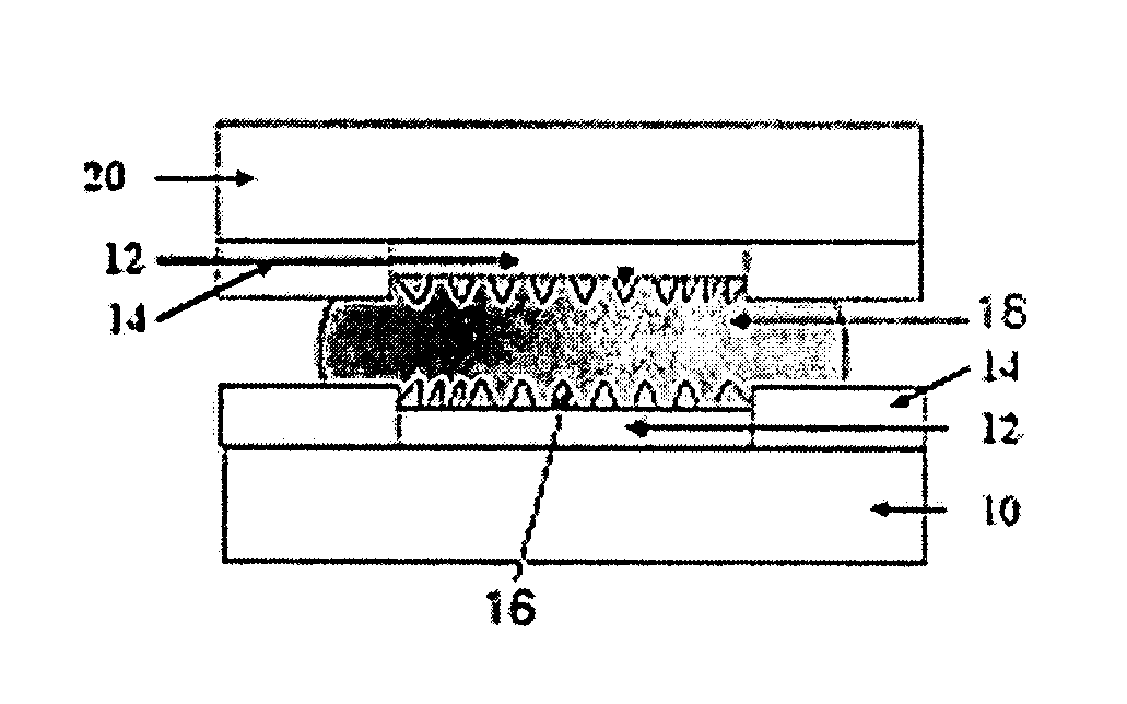
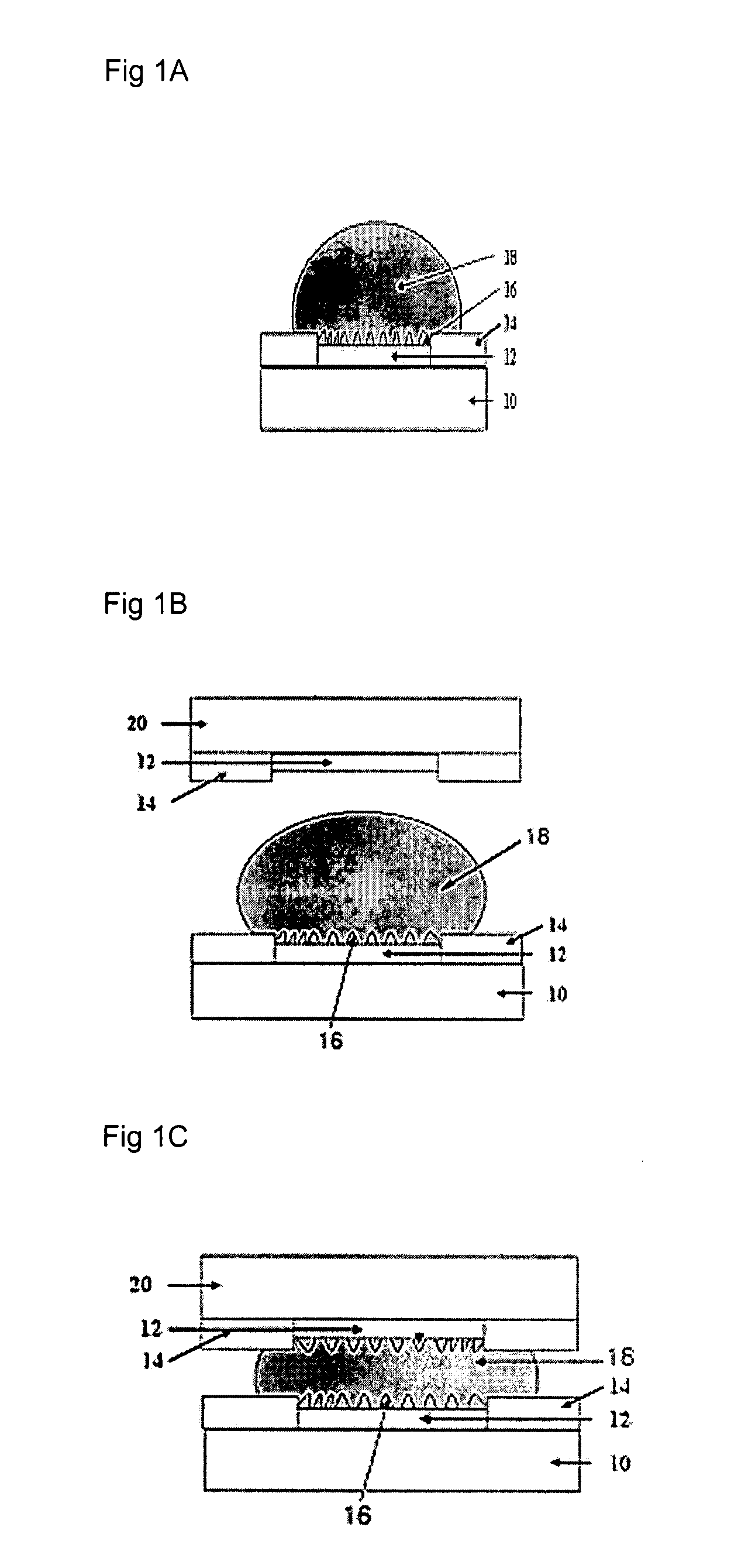
[0043]FIG. 1 is schematic views illustrating a process of connecting electronic parts, which are surface treated with copper or nickel layers according to the present invention. The solders used in the above process are Sn—Ag, Sn—Cu or Sn—Ag—Cu solders which have at least one selected from alloy elements such as Zn, Al, Be, Si, Ge and Mg added thereto. Alternatively, any one of the above elements may be vapor deposited on the copper or nickel layer of the electronic part in place of adding the alloy elements to the solders.

[0044]Metal surface treatment of a printed circuit board 10 comprises vapor deposition of copper or nickel by means of electro-plating, electroless plating, sputtering or lamination process. Also, any one selected from the above alloy elements can form a plating layer on the copper or nickel surface. After joining the lead-free solders by the reflowing process as shown in FIG. 1A and after aligning the package parts or the substrates 20 which were surface treated ...
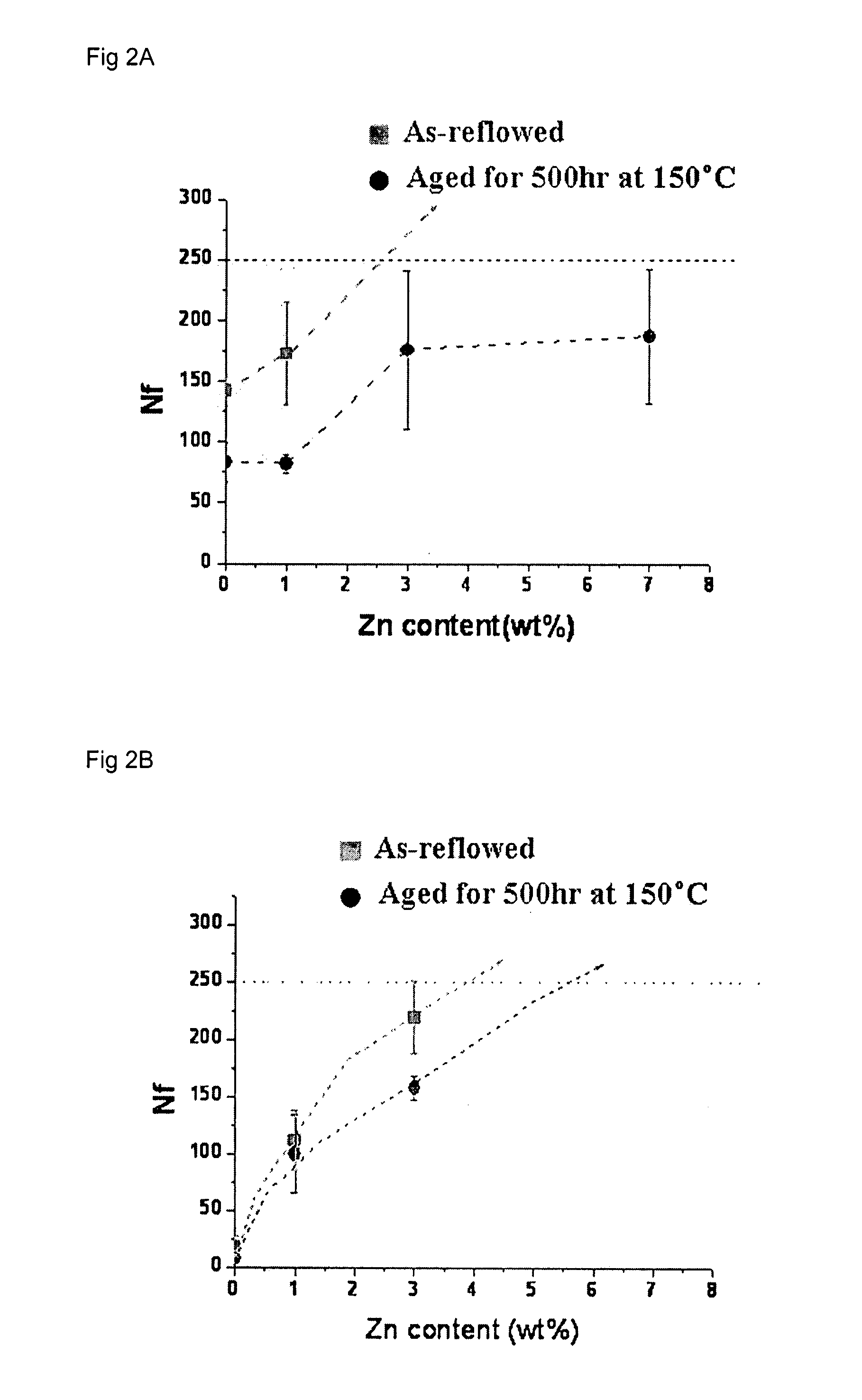

PUM

PropertyMeasurementUnit
Fractureaaaaaaaaaa

Abstract

Disclosed is a method of joining electronic package parts, comprising the steps of: reflowing lead-free solders containing alloy elements on top of each of the electronic package parts having a surface treated with copper or nickel; and mounting the surface treated electronic parts on the lead-free solders then reflowing the lead-free solders to generate intermetallic compound between the lead-free solders and the surface treated portion of each of the electronic parts.
Alternatively, the method of joining the electronic package parts according to the present invention comprises the steps of: forming a plating layer made of alloy elements on top of each of the electronic parts having a surface treated with copper or nickel and reflowing lead-free solders; and mounting the surface treated electronic parts on the lead-free solders then reflowing the lead-free solders to allow the alloy elements contained in the plating layer to be diffused into the lead-free solders and generate intermetallic compound between the lead-free solders and the surface treated portion of each of the electronic parts.
The present invention can prevent brittle fracture of the electronic package parts by deriving alteration of the intermetallic compounds generated from existing lead-free solders when the electronic package parts of electronic devices are solder joined together, thereby ensuring reliability of the electronic devices.

Description

BACKGROUND OF THE INVENTION[0001]This application claims priority to Korean Patent Application No. 2007-0030556, filed on Mar. 28, 2007, in the Korean Intellectual Property Office, the entire contents of which are hereby incorporated by reference.[0002]1. Field of the Invention[0003]The present invention relates to a method of joining electronic package capable of preventing brittle fracture, more particularly, to a method of joining separate electronic package parts (hereinafter, often referred to as “electronic parts”) for prevention of brittle fracture by using lead-free solders in joining the electronic parts having surfaces treated with copper or nickel, and / or forming a plating layer made of alloy elements on top of each of the electronic parts having a surface treated with copper or nickel then reflowing lead-free solders so as to alter phase of intermetallic compound generated at sites of joining each of the electronic parts and the lead-free solders.[0004]2. Description of ...

Claims


Application Information

Patent Timeline
IPC IPC(8): B23K31/02B23K1/00
CPCB23K1/0016B23K2201/40B23K2203/18H01L2224/13H05K3/3463H01L2224/8181H01L2224/16503H05K3/244B23K2101/34B23K2101/40B23K2103/18H01L24/03H01L24/05H01L24/11H01L24/13H01L24/81H01L2224/0401H01L2224/0554H01L2224/0557H01L2224/05571H01L2224/05573H01L2224/05647H01L2224/05655H01L2924/00014H01L2224/05599H01L2224/0555H01L2224/0556H01L23/48
Inventor YU, JINJEE, YOUNG-KUNKO, YONG-HO
Owner KOREA ADVANCED INST OF SCI & TECH
Why Eureka
Try Eureka