Ultraviolet detecting device and manufacturing method thereof, and ultraviolet quantity measuring apparatus

a technology of ultraviolet detecting device and manufacturing method, applied in the direction of solid-state device, radio-controlled device, instrument, etc., can solve the problems of inability to detect two wavelength ranges in separate forms, skin irritation, and danger of inducing skin cancer, so as to achieve the effect of miniaturization of ultraviolet quantity measuring apparatus and easy measuremen

Active Publication Date: 2008-10-02
LAPIS SEMICON CO LTD
View PDF1 Cites 22 Cited by
  • Summary
  • Abstract
  • Description
  • Claims
  • Application Information

AI Technical Summary

Benefits of technology

[0021]Advantageous effects can be obtained in that ultraviolet information can easily be measured by an ultraviolet quantity measuring apparatus equipped with the above ultraviole

Problems solved by technology

The UV-A wave causes skin to darken and reaches the inner or true skin, thus resulting in aging.
The UV-B wave causes skin irritation and is in danger of inducing skin cancer.
Promptly notifying a daily exposure dose of ultraviolet light presents an important challenge in terms of hu

Method used


Image

  • Ultraviolet detecting device and manufacturing method thereof, and ultraviolet quantity measuring apparatus
  • Ultraviolet detecting device and manufacturing method thereof, and ultraviolet quantity measuring apparatus
  • Ultraviolet detecting device and manufacturing method thereof, and ultraviolet quantity measuring apparatus

Examples


first preferred embodiment

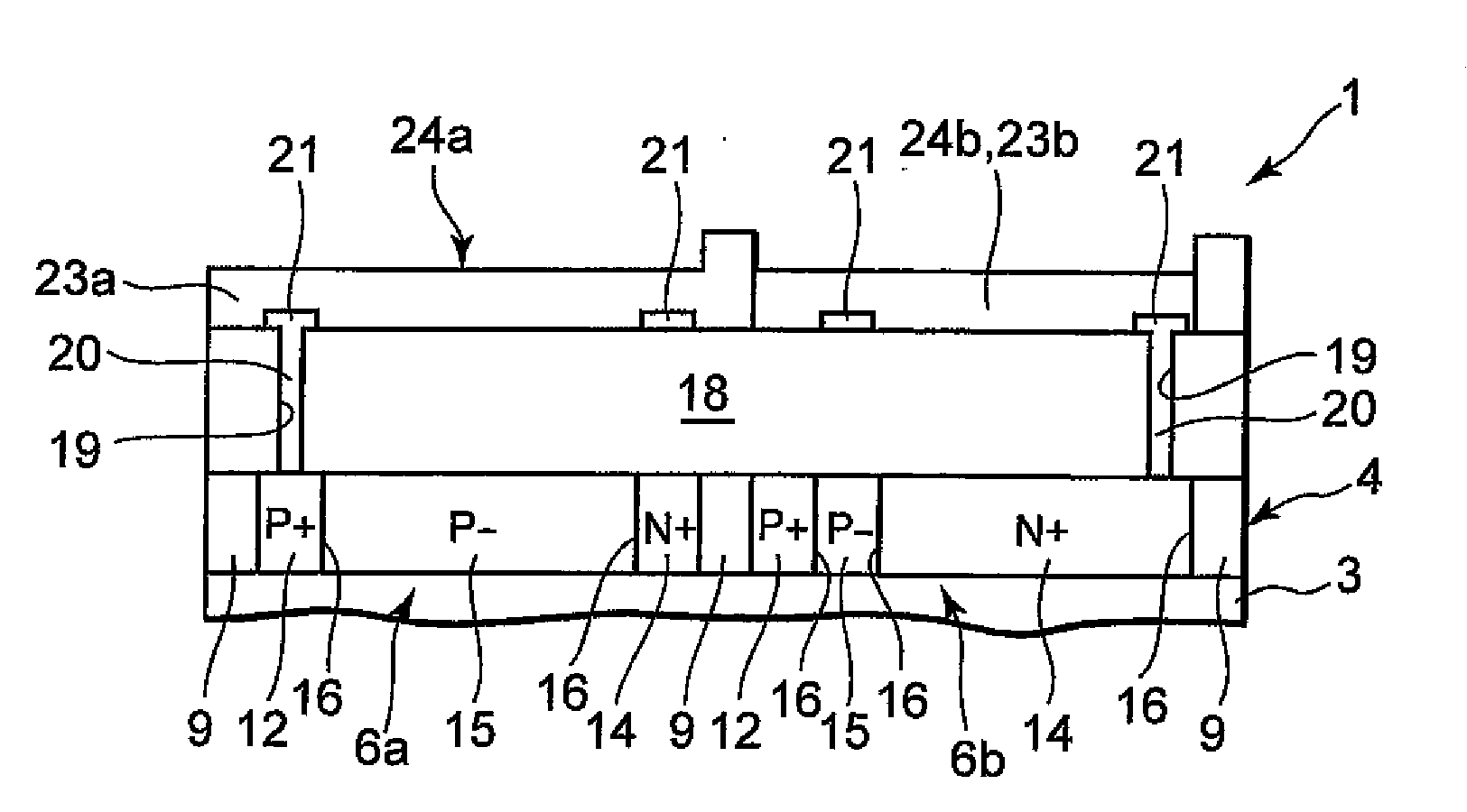
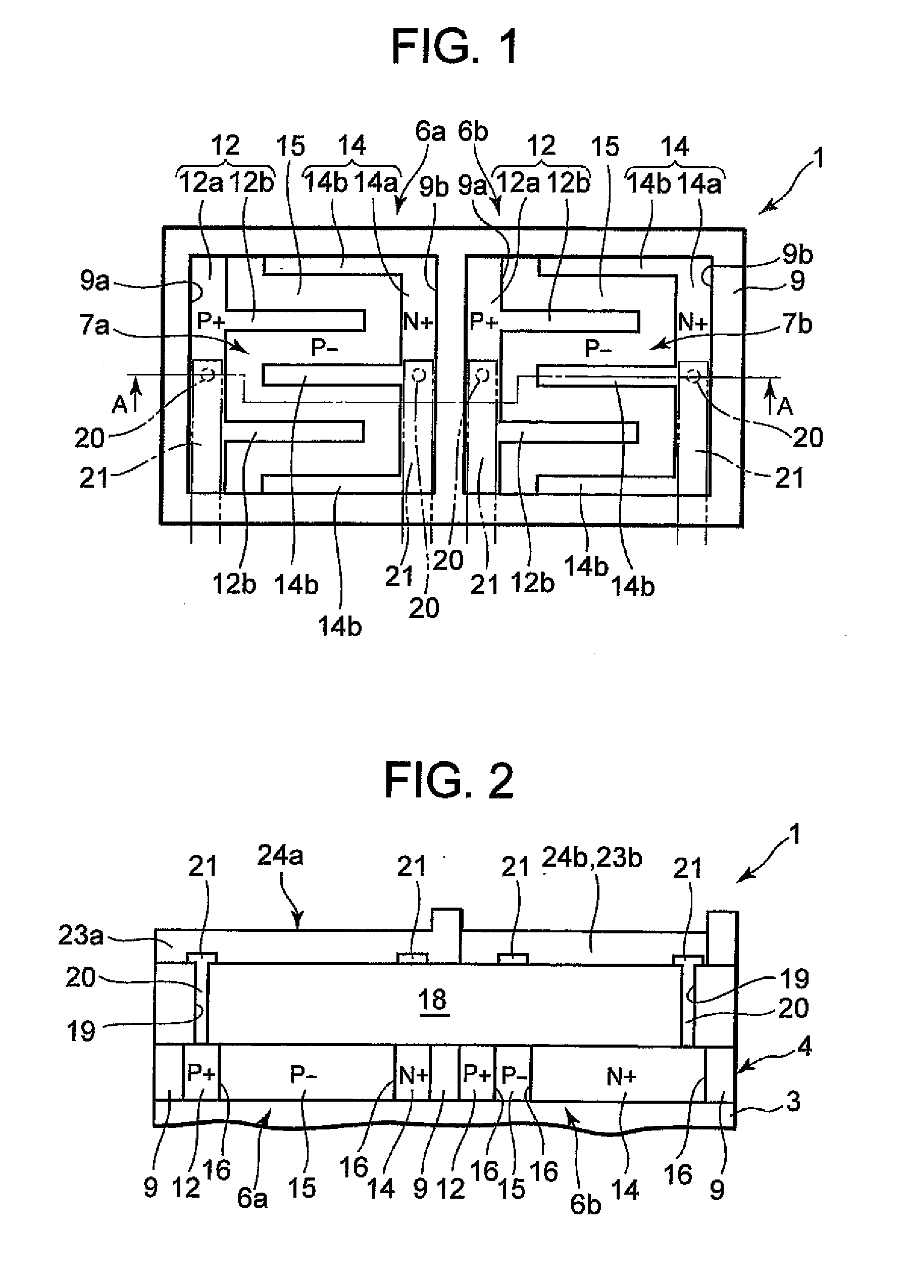
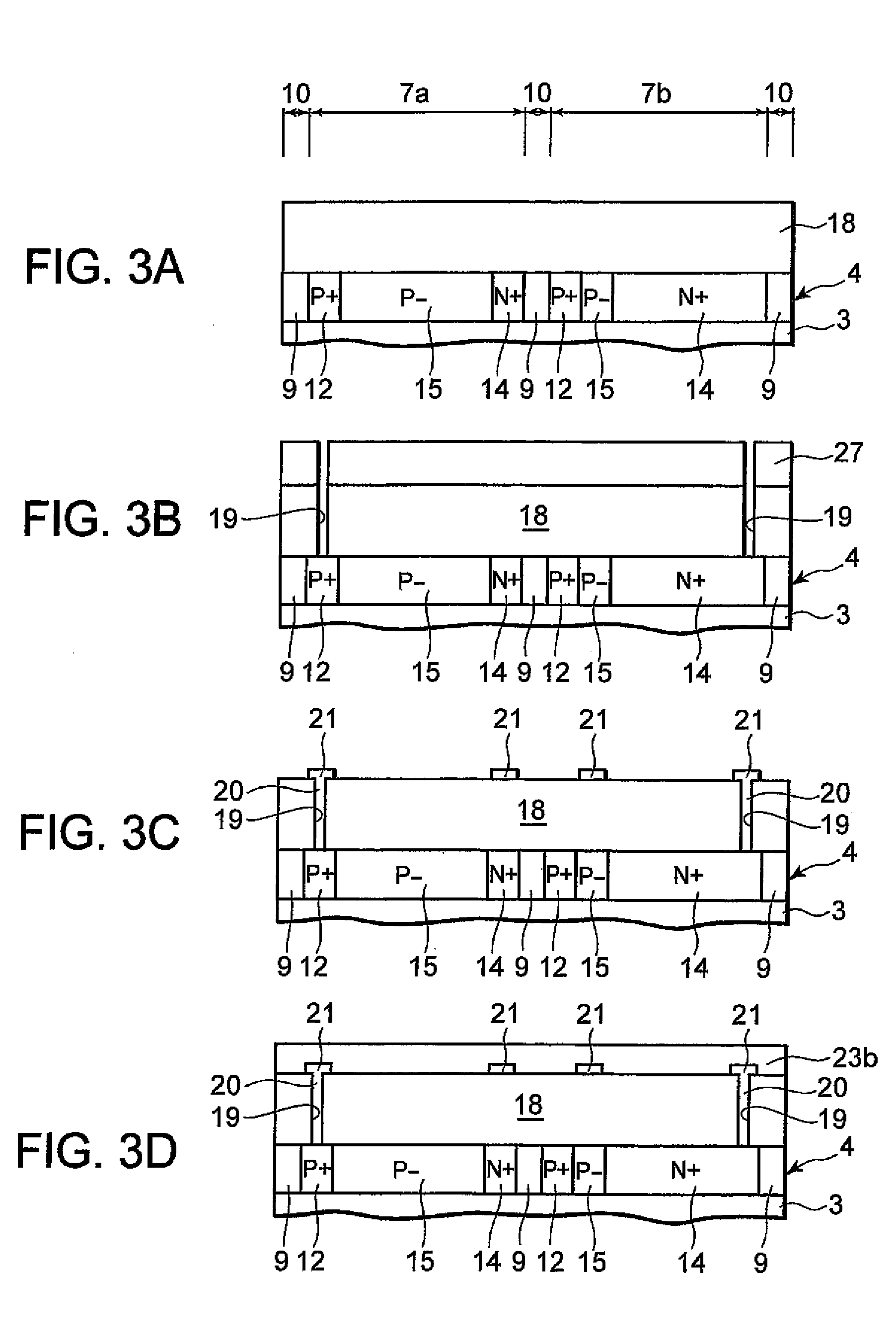
[0042]FIG. 1 is an explanatory diagram showing an upper surface of an ultraviolet detecting device according to a first embodiment, FIG. 2 is an explanatory diagram showing a section of the ultraviolet detecting device according to the first embodiment, and FIGS. 3A to 3D and FIGS. 4A to 4C are explanatory diagrams showing a method for manufacturing the ultraviolet detecting device according to the first embodiment, respectively.

[0043]Incidentally, FIG. 2 is a sectional view taken along sectional line A-A of FIG. 1. FIG. 1 is shown in a state in which each layer above a silicon semiconductor layer shown in FIG. 2 is being eliminated.

[0044]In FIGS. 1 and 2, reference numeral 1 indicates an ultraviolet detecting device which comprises lateral PN-junction type first and second photodiodes 6a and 6b formed in a silicon semiconductor layer 4 made of thin monocrystalline silicon (Si), of a semiconductor wafer having an SOI structure in which the silicon semiconductor layer 4 is formed on ...

second preferred embodiment

[0100]FIG. 10 is an explanatory diagram showing a section of an ultraviolet detecting device according to a second embodiment, and FIGS. 11A to 11D and FIGS. 12A to 12B are respectively explanatory diagrams showing a method for manufacturing the ultraviolet detecting device according to the second embodiment.

[0101]Incidentally, FIG. 10 is a sectional view shown in section similar to FIG. 2 showing the first embodiment. Its upper surface is similar to FIG. 1 showing the first embodiment. The same reference numerals are attached to portions or elements similar to those in the first embodiment and the description thereof will therefore be omitted.

[0102]A first filter layer 24a is formed on a first photodiode 6a of the present embodiment with an interlayer insulating film 18 interposed therebetween.

[0103]A filter layer of stacked structure comprising a second filter layer 24b and the first filter layer 24a is formed over a second photodiode 6b with the interlayer insulating film 18 inte...

third preferred embodiment

[0121]FIG. 14 is a block diagram showing an ultraviolet quantity measuring apparatus according to a third embodiment, and FIG. 15 is a flow chart showing an ultraviolet information measuring process of the third embodiment, respectively.

[0122]Incidentally, the same reference numerals are attached to portions or elements similar to those in the first embodiment, and their explanations are omitted.

[0123]As shown in FIG. 14, the ultraviolet quantity measuring apparatus 31 of the present embodiment comprises a first photodiode 6a which selectively outputs the quantities of ultraviolet light lying in wavelength ranges of UV-A and UV-B waves as current values according to the thicknesses of a first filter layer 24a and a silicon semiconductor layer 4, a second photodiode 6b which selectively outputs the quantity of ultraviolet light lying in the wavelength range of the UV-A wave as a current value according to the thicknesses of a second filter layer 24b and the silicon semiconductor laye...


PUM


Abstract

The present invention provides an ultraviolet detecting device which comprises a silicon semiconductor layer having a thickness ranging from greater than or equal to 3 nm to less than or equal to 36 nm, which is formed over an insulating layer, lateral PN-junction type first and second photodiodes formed in the silicon semiconductor layer, an interlayer insulating film formed over the silicon semiconductor layer, a first filter layer made of silicon nitride, which is formed over the interlayer insulating film provided over the first photodiode and causes light lying in a wavelength range of an UV-B wave or higher to pass therethrough, and a second filter layer made of silicon nitride, which is formed over the interlayer insulating film provided over the second photodiode and allows light lying in a wavelength range of an UV-A wave or higher to pass therethrough.

Description

BACKGROUND OF THE INVENTION [0001]The present invention relates to an ultraviolet detecting device using photodiodes that produces currents in light and its manufacturing method, and an ultraviolet quantity measuring apparatus.[0002]In a conventional ultraviolet receiving or detecting device, photodiodes laterally disposed opposite to each other in such a manner that comb teeth portions of both an N+ diffusion layer in which an N-type impurity is diffused in a high concentration and which is shaped in the form of an “E”-shaped comb type, and a P+ diffusion layer in which a P-type impurity is diffused in a high concentration and which is shaped in the form of “π”-shaped comb type, are brought into engagement with each other, are formed in a silicon semiconductor layer with an N-type impurity diffused therein in a low concentration, of a semiconductor wafer of SOI (Silicon On Insulator) structure in which a silicon semiconductor layer of an about 150 nm-thick is formed on a silicon su...

Claims


Application Information

Patent Timeline
IPC IPC(8): H01L31/0203H01L31/18
CPCH01L27/144H01L31/105H01L31/02162G01R1/42
Inventor MIURA, NORIYUKICHIBA, TADASHI
Owner LAPIS SEMICON CO LTD
Why Eureka
Try Eureka