

Liquid crystal device, pixel circuit, active matrix substrate, and electronic apparatus
a liquid crystal device and memory circuit technology, applied in the direction of electric digital data processing, instruments, computing, etc., can solve the problems of unrealistic operation of the memory circuit provided in each of the pixels with a negative power supply, inability to employ the liquid crystal device that uses the memory circuit, and difficulty in performing ideal operation, etc., to achieve accurate inversion of applied voltage, simple circuit configuration, and simple control
- Summary
- Abstract
- Description
- Claims
- Application Information
AI Technical Summary
Benefits of technology
Problems solved by technology
Method used
Image

Examples
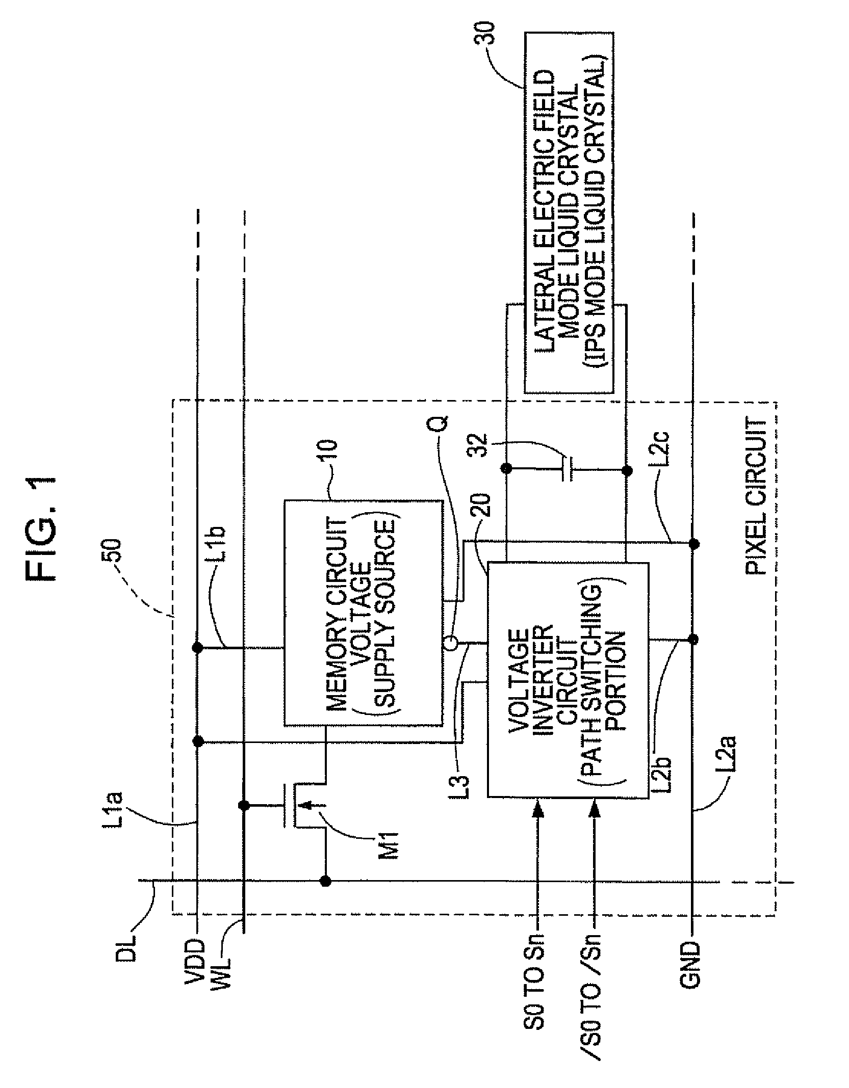
first embodiment
of Line Sequential Driving in Writing Display Data
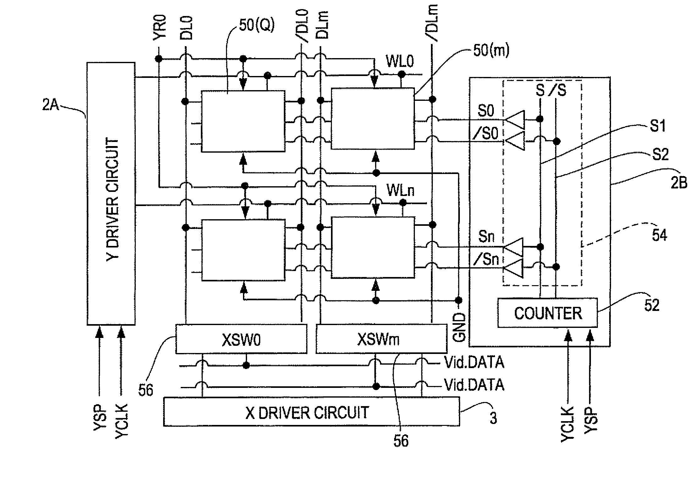
[0136]FIG. 9 is a block diagram that illustrates an operation in the liquid crystal device that performs line sequential driving in writing display data according to the embodiment of the invention. As shown in the drawing, the liquid crystal device includes the scanning line driving circuit 2, the data line driving circuit 3, and the image display area 5 that includes the plurality of pixel circuits (500 to 50 m). Note that the description of the configuration of the liquid crystal device described with reference to FIG. 6 will be omitted. The scanning line driving circuit 2 is driven by the scanning line driving circuit start signal YSP and sequentially outputs a “H (high)” level signal to the scanning lines (WL) at a timing of the Y clock signal YCLK. In addition, the scanning line driving circuit 2 outputs the switch control signals S0 to Sn, / S0 to / Sn that will be supplied to the voltage inverter circuit 20 included in each of ...
second embodiment
of Line Sequential Driving in Writing Display Data
[0147]FIG. 11 is another operation timing chart in regard to the writing operation of display data and the update of display data in the liquid crystal device that performs line sequential driving in writing display data according to the embodiment of the invention. In the present embodiment, the waveforms of the switch control signals S0, / S0 are different from those shown of FIG. 10.
[0148]That is, in the liquid crystal device that performs line sequential driving in writing display data according to the embodiment of the invention, when the reset signals rst0 to rstn are supplied in a period when data are sequentially written to the pixel circuits connected to one of the scanning lines WL0 to WLn, in a period when the next display data is written to the memory circuit in the pixel circuit, the input of the voltage inverter circuit is made to enter a floating state by means of a control using the reset signals rst0 to rstn to thereb...
third embodiment
[0157]In the present embodiment, the circuit configuration that suppresses a feedthrough current (Ipeak) in the voltage inverter circuit 20 will be described.
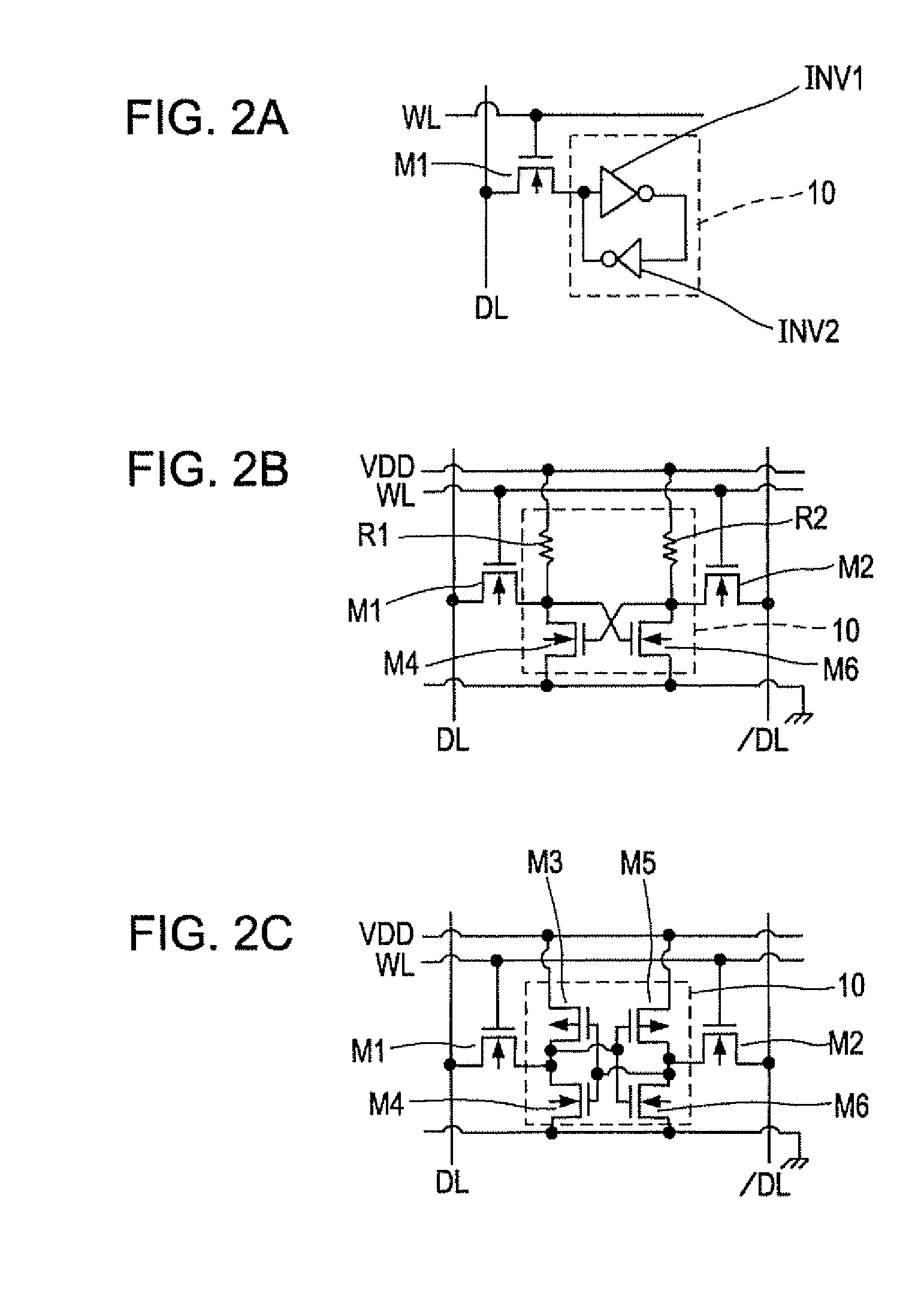
[0158]FIG. 14A to FIG. 14C are views, each of which illustrates the circuit configuration and operation of a voltage inverter circuit that has a device to suppress a feedthrough current (Ipeak). FIG. 14A is a circuit diagram that shows the circuit configuration. FIG. 14B is a timing chart that shows the operation of the circuit shown in FIG. 14A. FIG. 14C is a timing chart that shows the operation of a circuit that does not have a device to suppress a feedthrough current according to a comparative embodiment. In FIG. 14A to FIG. 14C, the same reference numerals are assigned to the same components as those shown in the above described drawings.
[0159]The voltage inverter circuit 20 shown in FIG. 3 has such a configuration that two MOS transistors (M7 and M8, or M9 and M10) are connected in series between the voltage supply end (Q...
PUM
 Abstract
Description
Claims
Application Information