Laser beam formatting module and method for fabricating semiconductor dies using same

a semiconductor and die technology, applied in the field of semiconductor fabrication, can solve the problems of reducing image quality, reducing image quality, and generating excess hea

Active Publication Date: 2008-10-02
GLOBALFOUNDRIES US INC
View PDF2 Cites 11 Cited by
  • Summary
  • Abstract
  • Description
  • Claims
  • Application Information

AI Technical Summary

Problems solved by technology

Light that is significantly shorter or longer than the desired wavelength (out-of-band radiation) may not be useful to the lithographic process, and may have the undesirable effect of reducing image quality, and producing excess heat.

Method used


Image

  • Laser beam formatting module and method for fabricating semiconductor dies using same
  • Laser beam formatting module and method for fabricating semiconductor dies using same
  • Laser beam formatting module and method for fabricating semiconductor dies using same

Examples


Embodiment Construction

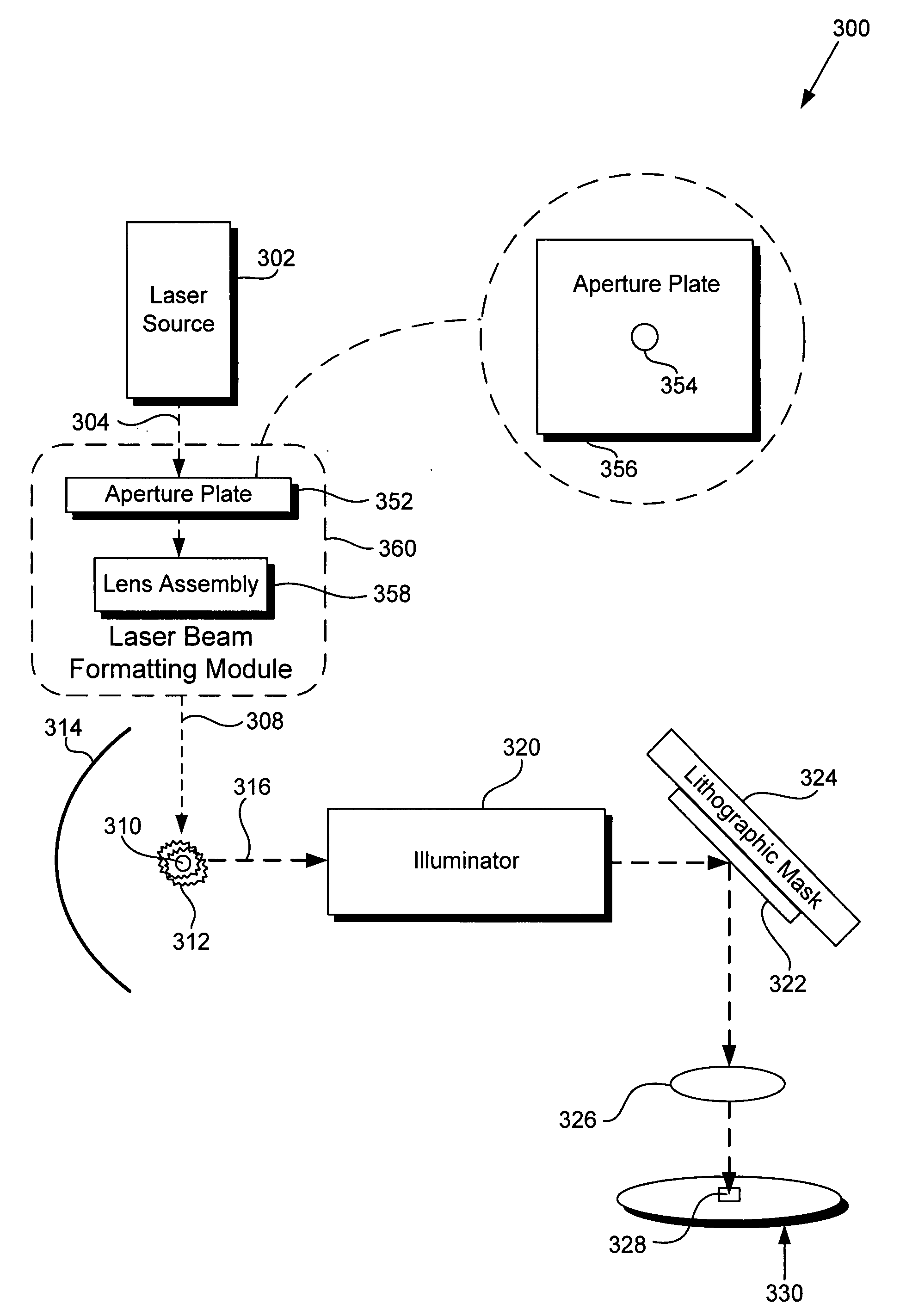
[0010]The present invention is directed to a laser beam formatting module and method for fabricating semiconductor dies using same. The following description contains specific information pertaining to the implementation of the present invention. One skilled in the art will recognize that the present invention may be implemented in a manner different from that specifically discussed in the present application. Moreover, some of the specific details of the invention are not discussed in order not to obscure the invention.

[0011]The drawings in the present application and their accompanying detailed description are directed to merely exemplary embodiments of the invention. To maintain brevity, other embodiments of the present invention are not specifically described in the present application and are not specifically illustrated by the present drawings.

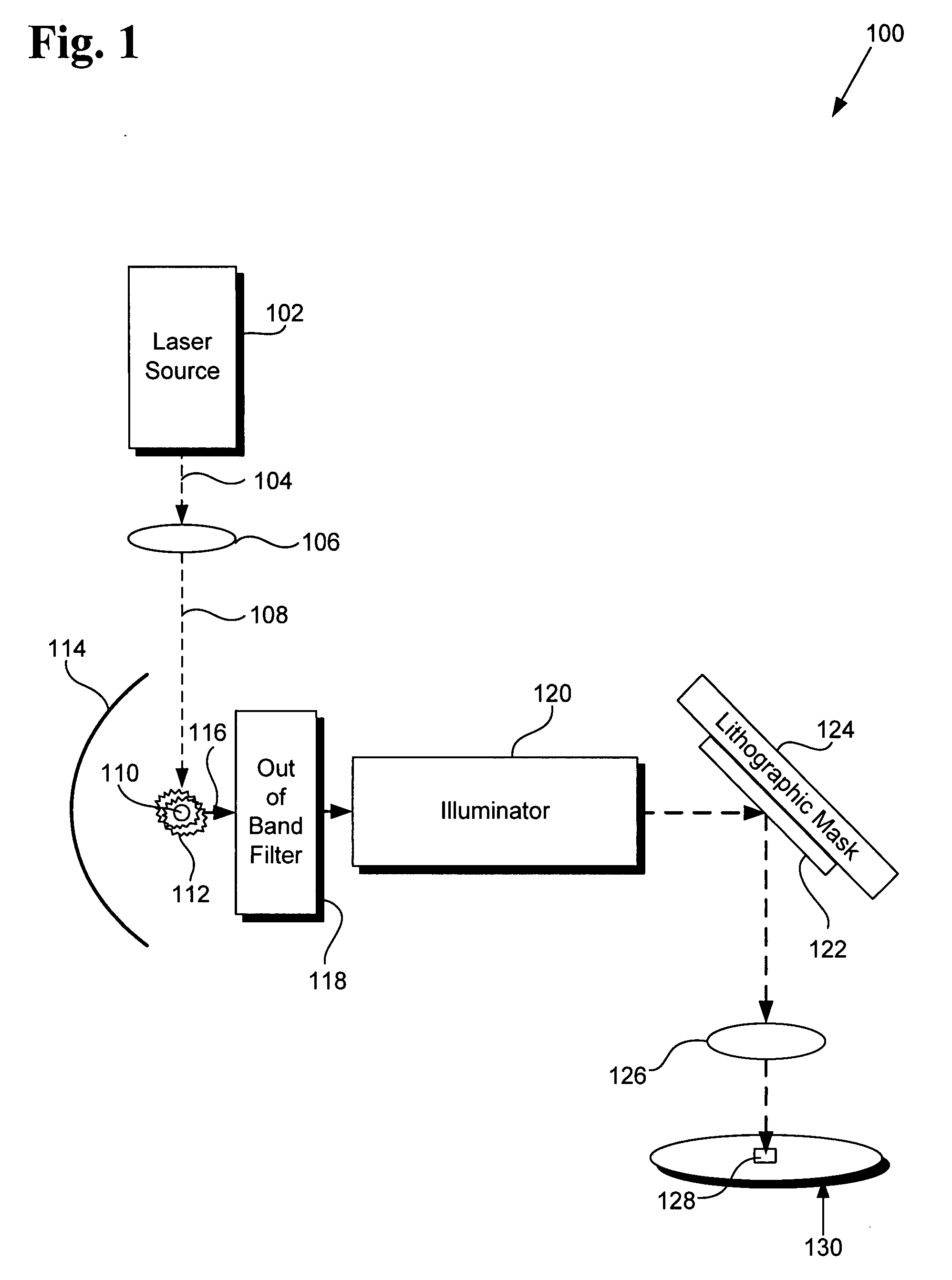
[0012]FIG. 1 illustrates a diagram of a conventional lithographic system utilizing a laser-produced plasma (LPP) light source. FIG. 1 i...


PUM


Abstract

According to one exemplary embodiment, a laser beam formatting module for use in a lithographic system to fabricate a semiconductor wafer comprises an aperture plate having, for example, a circular aperture and capable of being situated between a laser source and a target, and a lens assembly, in a light path between the aperture plate and the target. The laser beam formatting module can produce a substantially uniform laser beam intensity across a target during fabrication of a semiconductor wafer in a laser-produced plasma (LPP) lithographic process using, for example, extreme ultraviolet light (EUV). In one embodiment, a laser beam formatting module improves energy conversion efficiency, reduces out-of-band radiation emission, avoids heating of reflective optics, and eliminates the need for an out-of-band radiation filter.

Description

TECHNICAL FIELD[0001]The present invention is generally in the field of semiconductor fabrication. More particularly, the invention is in the field of lithographic patterning of semiconductor wafers.BACKGROUND ART[0002]During semiconductor wafer fabrication, light can be utilized in a lithographic process to enable transfer of very small lithographic patterns, such as nanometer-scale lithographic patterns, from a lithographic mask to a semiconductor wafer. In EUV lithography, for example, a laser-produced plasma (LPP) serves as a lithographic light source, at extreme ultraviolet (EUV) wavelengths. As a result of LPP light source emission, a pattern formed on a lithographic mask can be transferred to a semiconductor wafer by exposing a photoresist formed on the semiconductor wafer to the image of the lithographic mask.[0003]A conventional method for producing LPP light emission in a lithographic system involves use of a focusing lens situated between the laser source and the target t...

Claims


Application Information

Patent Timeline
Patent Type & Authority Applications(United States)
IPC IPC(8): G03B27/42G02B27/42G03B27/52
CPCB82Y10/00G03F7/70033H05G2/001
Inventor LAFONTAINE, BRUNO M.WOOD, OBERT REEVES
Owner GLOBALFOUNDRIES US INC
Why Eureka
Try Eureka