

Liquid Crystal Display Device with Evaluation Patterns Disposed Thereon, and Method for Manufacturing the Same
- Summary
- Abstract
- Description
- Claims
- Application Information
AI Technical Summary
Benefits of technology
Problems solved by technology
Method used
Image

Examples
embodiment 1
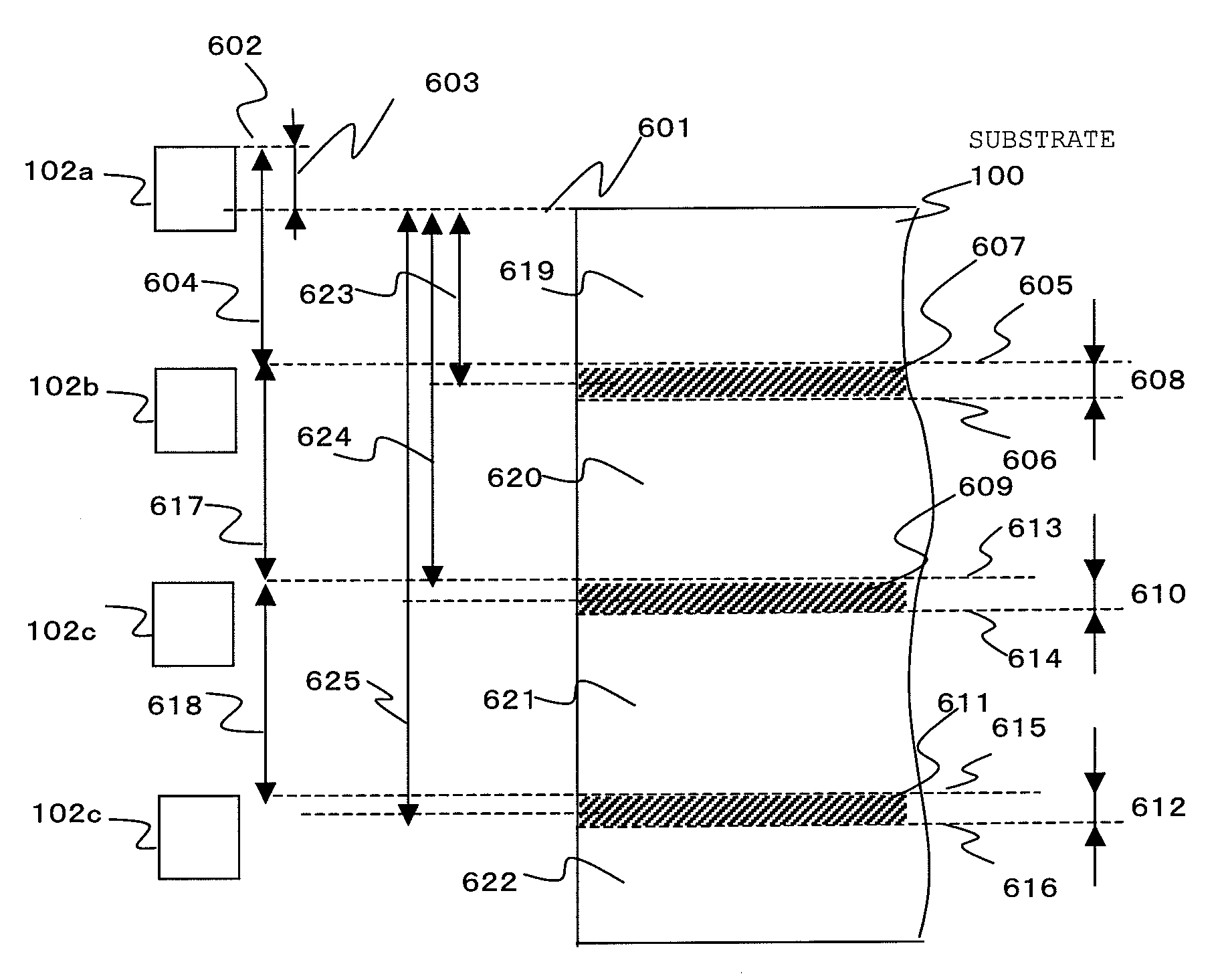
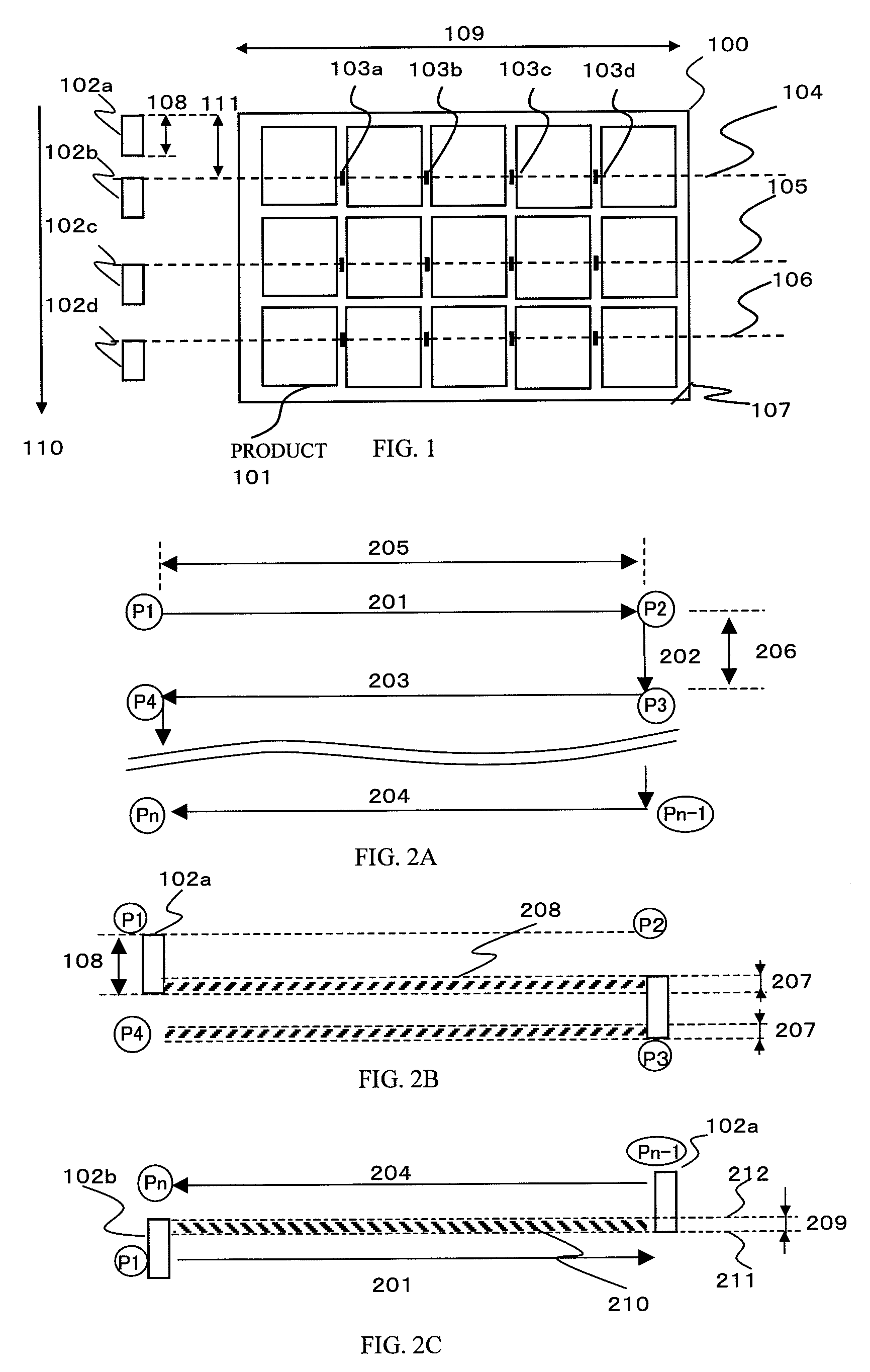
[0069]FIG. 1 shows a method for disposing evaluation TEGs in the present invention.
[0070]The orientation of a substrate 100 is regulated by an orientation flat 107. Panels 101 are disposed upon this substrate 100. The number of panels disposed upon the substrate is arbitrary. FIG. 1 merely shows a schematic example illustrating a concept, and does not limit factors such as the number of panels. These panels are exposed by the exposure heads 102a, 102b, 102c, and 102d of a piece of exposure equipment. Also with regard to the number of exposure heads, FIG. 1 illustrates the case wherein exposure is conducted with four heads, but the number of heads is not limited to four. These exposure heads are arranged according to a fixed spacing 111. The respective exposure heads conduct a single exposure over a width equal to the head width (HW) 108, as the stage moves in the main scan direction 109. When a single scan ends, the stage moves in the sub scan direction. As a result, the positions o...
embodiment 2
[0107]In the first embodiment, a method was disclosed wherein problems in exposure head alignment are detected by measuring the line widths of evaluation TEGs. The second embodiment will disclose a method wherein problems in exposure head alignment are detected by measuring the resistance of the evaluation TEGs.
[0108]If film thickness is nearly uniform, then line width and resistance exist in an inverse relationship. Consequently, it is possible to configure in advance a reference value for resistance fluctuation similar to line width fluctuation for the respective TEGs for resistance measurement to be hereinafter described.
[0109]Since the method of disposing the evaluation TEGs on the substrate is the same, the shape and other features of the TEGs for resistance measurement will now be described.
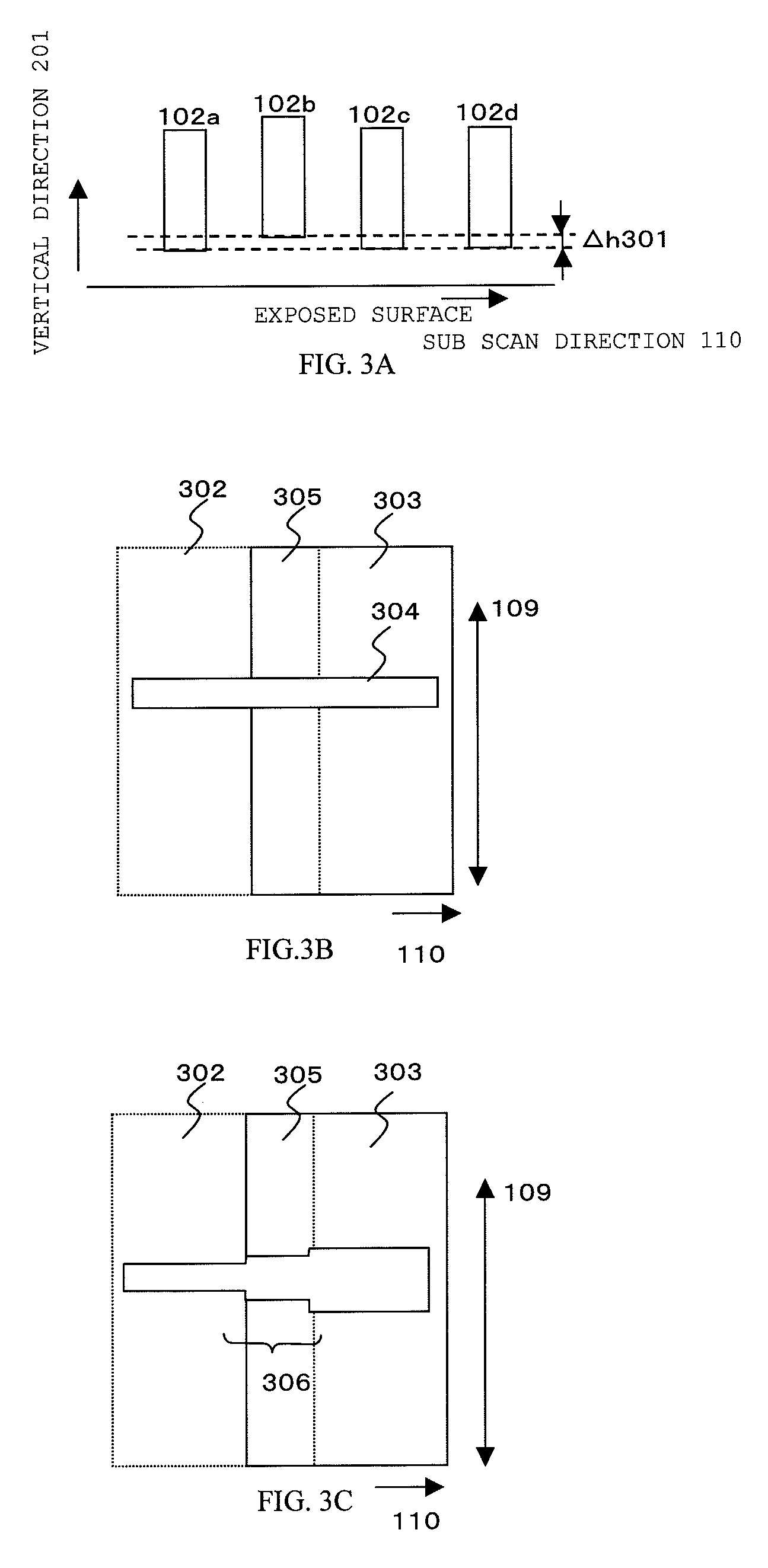
[0110]The TEG shown in FIG. 15 detects irregularities in head positioning in the vertical direction as described with reference to FIG. 3A, as well as irregularities in head positioning in ...
embodiment 3
[0129]In the first embodiment, an embodiment was described wherein TEGs are placed at the head exposure area boundaries. Here, however, an example will be described wherein evaluation patterns are also disposed at the returning boundaries within the areas exposed by the same head. In addition, while in the first embodiment the evaluation patterns were disposed on the scribe lines, herein an embodiment will be described wherein evaluation patterns are also disposed in the products. When the evaluation patterns are disposed in the products, the locations of the head exposure area boundaries and the returning boundaries are known from the positions of the evaluation patterns, even after cutting the products from the substrate. For this reason, this method has the merit of making it easier to conduct defect analysis or other tests after the fact. The above will be described in conjunction with FIG. 23. The all-encompassing rectangle 2300 is a substrate subjected to exposure. When an ori...
PUM
| Property | Measurement | Unit |
|---|---|---|
| Angle | aaaaa | aaaaa |
| Length | aaaaa | aaaaa |
| Electrical resistance | aaaaa | aaaaa |
Abstract
Description
Claims
Application Information