
Wiring board and method of manufacturing the same

a technology of wiring board and core board, which is applied in the direction of conductive pattern formation, circuit inspection/indentification, etc., can solve the problems of reducing process precision and thinness of the core board serving as the base of the wiring board

Active Publication Date: 2008-10-09
SHINKO ELECTRIC IND CO LTD
View PDF8 Cites 28 Cited by
  • Summary
  • Abstract
  • Description
  • Claims
  • Application Information

AI Technical Summary

Benefits of technology

[0012]A specific object of the present invention is to provide a method of manufacturing a wiring board and the wiring board, which enables the wiring board to be thinned and improves precision in alignment.
[0015]According to the present invention, a method of manufacturing a wiring board is provided which enables the wiring substrate to be thinned and improves precision in alignment.

Problems solved by technology

However, when trying to make the core board further thinner in the aforementioned build-up method, there is a problem in thickness of the core board serving as a base of the wiring board.
However, since adhesion is not strong between the support plate made of metal and the build-up layer made of resin, a countermeasure is needed to improve adhesion.
Accordingly, it is difficult to recognize the alignment mark in positioning the wiring board, and thus reliability in process precision may decrease.

Method used


Image

  • Wiring board and method of manufacturing the same
  • Wiring board and method of manufacturing the same
  • Wiring board and method of manufacturing the same

Examples


embodiment 1

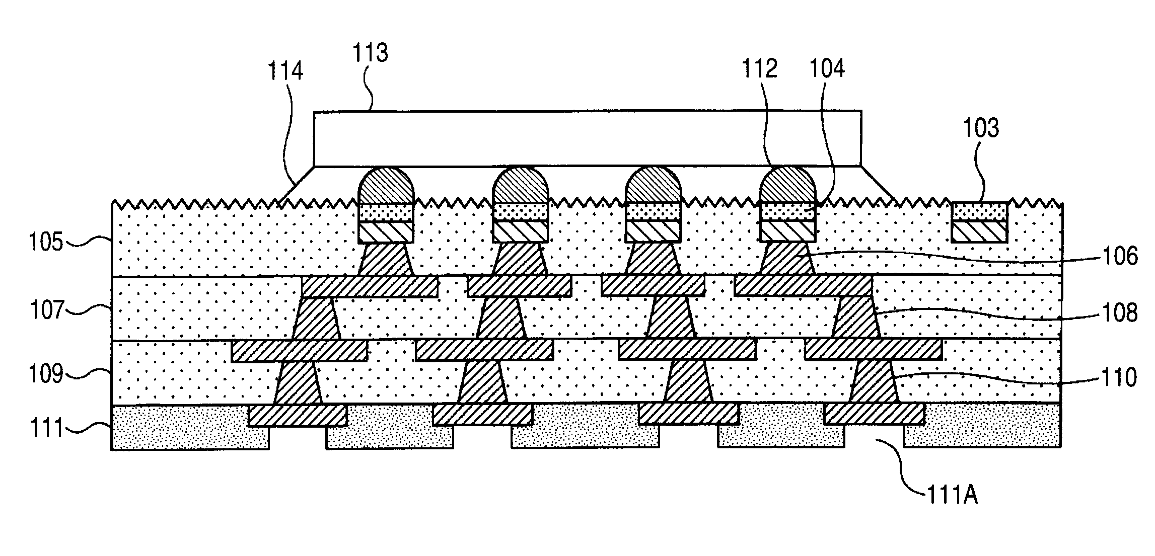
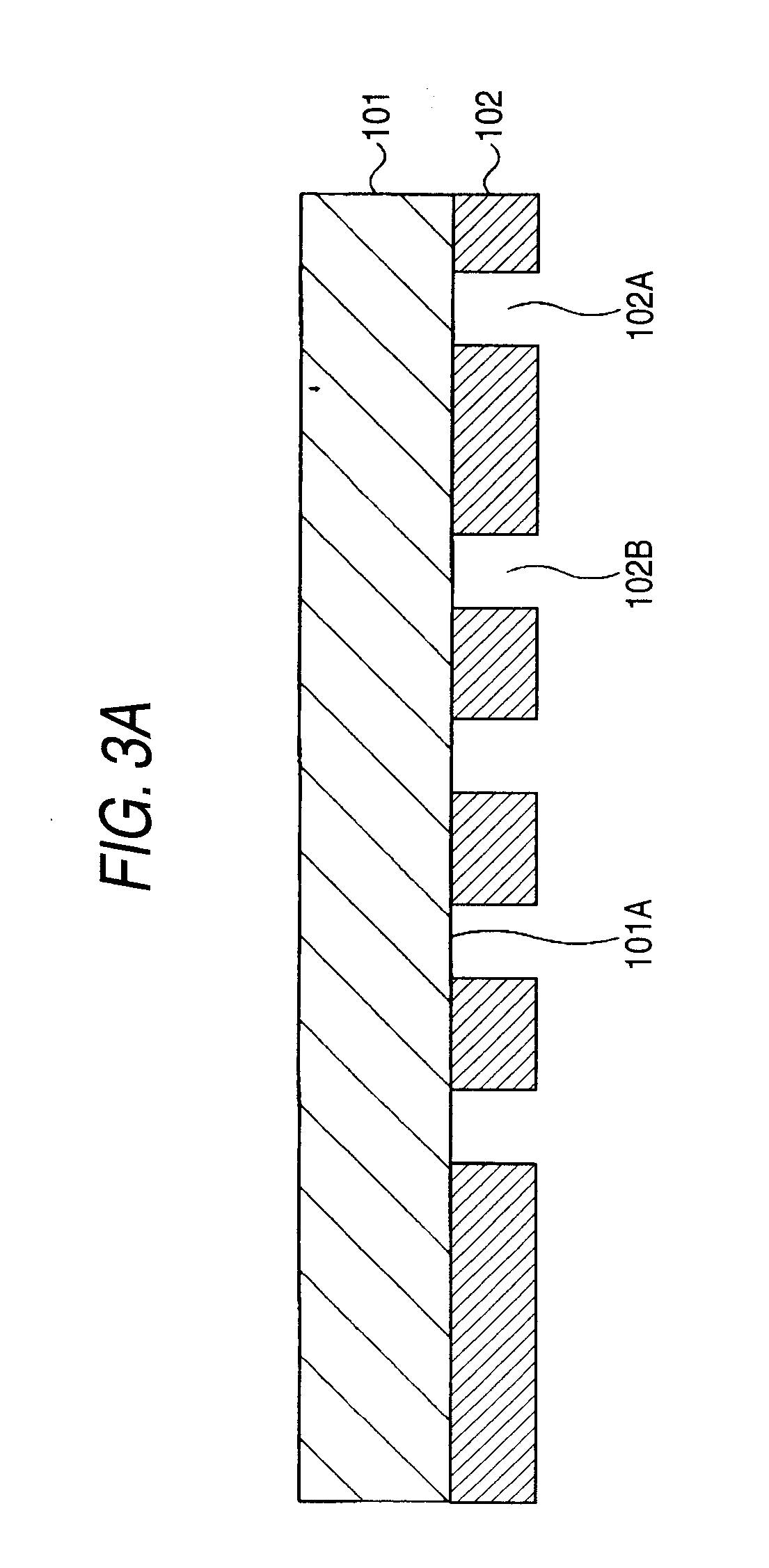
[0053]FIGS. 3A to 3I are diagrams sequentially illustrating a method of manufacturing a wiring board (electronic device) according to Embodiment 1. In the figures, the same reference numerals are given to the above-described parts, description of which may be omitted (the same is applied to the following embodiments and figures).

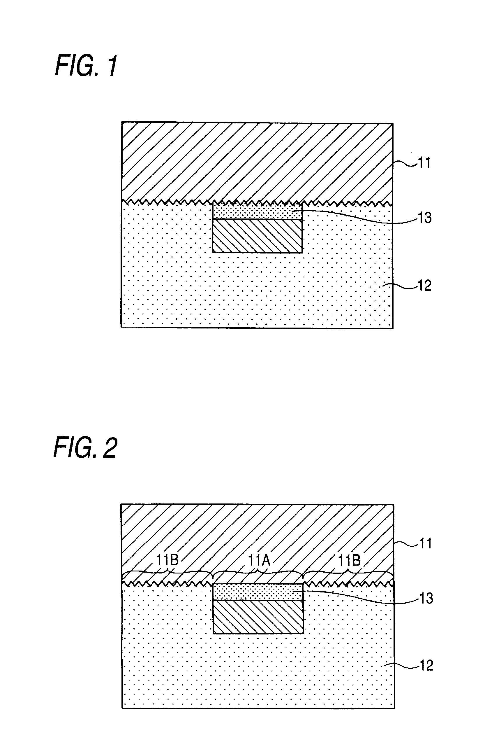
[0054]In the process shown in FIG. 3A, a mask pattern 102 having openings 102A and 102B is formed on a support plate 101, which is formed of Cu film by electroplating, by photolithography using resist. The surface of the support plate 101A is in the general metal plate state, and the surface is a non-rough surface (first area) 101A having Ra of 100 nm or less. The support plate is not limited to metal film (Cu film), but the general metal plate may be used as the support plate.

[0055]In the process shown in FIG. 3B, an alignment mark (conductive pattern) 103 and an electrode pad (conductive pattern) 104 are formed to come into contact with the surface (first ...

embodiment 2

[0068]FIGS. 4A to 4E are diagrams sequentially illustrating a method of manufacturing a wiring board (electronic device) according to Embodiment 2.

[0069]In the process shown in FIG. 4A, a surface of a support plate 201 made of metal such as Cu is subjected to a wet treatment using chemicals containing organic acid such as formic acid, and a rough surface (second area) 201B is formed. In this case, Ra that is surface roughness of the second area 201B is preferably 200 nm to 600 nm (e.g., 400 nm).

[0070]In the process shown in FIG. 4B, a mask pattern 202 having openings 202A and 202B is formed on the second area 201B of the support plate 201.

[0071]In the process shown in FIG. 4C, the second area 201B exposed from the openings 202A and 202B of the mask pattern 202 is smoothened by a wet treatment using chemicals containing, for example, sodium persulfate to form a non-rough surface (first area 201A). For example, Ra that is surface roughness of the first area 201A is preferably 100 nm o...

embodiment 3

[0076]In Embodiment 1 and Embodiment 2, both of the alignment mark and the electrode pad are formed corresponding to the non-rough surface, but the invention is not limited thereto. For example, at least the alignment mark of the alignment mark and the electrode pad may be formed corresponding to the non-rough surface, and the electrode pad may be formed corresponding to the rough surface, as described below.

[0077]FIGS. 5A to 5G are diagrams illustrating a method of manufacturing a wiring board (electronic device) according to Embodiment 3 of the invention.

[0078]In the process shown in FIG. 5A, a surface of a support plate 301 made of metal such as Cu is subjected to a wet treatment using chemicals containing organic acid such as formic acid, and a rough surface (second area) 301B is formed. In this case, Ra that is surface roughness of the second area 301B is preferably 200 nm to 600 nm (e.g., 400 nm).

[0079]In the process shown in FIG. 5B, a mask pattern 302 having an opening 302A ...


PUM

PropertyMeasurementUnit
surface roughnessaaaaaaaaaa
Raaaaaaaaaaa

Abstract

In a method of manufacturing a wiring board, the method includes: (i) forming a plurality of conductive patterns to come into contact with a support plate; (ii) forming a resin layer to cover the plurality of conductive patterns and to come into contact with the support plate; (iii) forming another conductive pattern connected to at least one of the plurality of conductive patterns; and (iv) removing the support plate. A first area of the support plate coming into contact with at least one of the plurality of conductive patterns in step (i) is different in surface roughness from a second area of the support plate coming into contact with the resin layer in step (ii).

Description

[0001]This application is based on and claims priority from Japanese Patent Applications No. 2007-101465, filed on Apr. 9, 2007, the entire contents of which are hereby incorporated by reference.BACKGROUND OF THE INVENTION[0002]1. Technical Field[0003]The present disclosure relates to a wiring board having an electrode pad and an alignment mark and a method of manufacturing the wiring board.[0004]2. Background Art[0005]Various configurations of a wiring board (electronic device) have been proposed that mount components such as semiconductor chips. In recent years, there has been a significant demand for making a wiring board on which a semiconductor chip is mounted thin in thickness and small in size, as the semiconductor chip is made thin in thickness and small in size.[0006]As a method of manufacturing the wiring board to be thin in thickness, for example, a so-called build-up method has been known. In the build-up method, a build-up layer (build-up resin) made of epoxy resin is s...

Claims


Application Information

Patent Timeline
Patent Type & Authority Applications(United States)
IPC IPC(8): H01B5/00H01R43/00
CPCH05K1/0269H05K1/113H05K3/205H05K3/382H05K3/4679H05K3/4682Y10T29/49126H05K2201/09918H05K2203/0346Y10T29/49165Y10T29/49155Y10T29/49224H05K2201/09781H01L2224/16225H01L2224/32225H01L2224/73204H01L2924/00011H01L2924/00014H01L2924/15174H01L2924/00H01L2224/0401H05K3/46
Inventor KODANI, KOTARONAKAMURA, JUNICHIKANEKO, KENTARO
Owner SHINKO ELECTRIC IND CO LTD
Learn More