Process and donor elements for transfering thermally sensitive materials to substrates by thermal imaging

a technology of thermal imaging and donor elements, which is applied in the direction of diffusion transfer process, thermography, instruments, etc., can solve the problems of high cost of organic transistors, severe degradation of organic semiconductors, and low cost of traditional transistors

Inactive Publication Date: 2005-09-29
EI DU PONT DE NEMOURS & CO
View PDF13 Cites 15 Cited by
  • Summary
  • Abstract
  • Description
  • Claims
  • Application Information

AI Technical Summary

Benefits of technology

[0024] The process and donor element of this invention are useful in the manufacture of thin film transistors and polymer light-emitting displays.

Problems solved by technology

While the same component densities as silicon transistors have not yet been achieved, the low cost of organic transistors means that they can be used in applications where high density is not required and traditional transistors are not economical.
If a photoresist is used during deposition, wet chemical etching after deposition is necessary, which may result in severe degradation of the organic semiconductor.
While easier and less expensive than the fabrication techniques required by silicon based transistors, such methods are still complex, slow, lack sufficient resolution, expose the device to deleterious heat and chemical processes, and are more expensive than necessary.
While facilitating the fabrication process, screen-printing and ink-jet printing do not provide sufficient resolution for certain applications.
In addition, it is also difficult to control the flatness and uniformity of the final film in ink-jet printing processes.
However, direct thermal printing of extremely thin films of semiconductors or light-emitting organic materials that are fragile and sensitive to perturbations (e.g., large temperature gradients, humidity, pressure or mechanical stress) has not been achieved.
Attempts to thermal transfer materials such as pentacene, fluorinated copper phthalocyanine, or organic light-emitting materials usually results in severe degradation and / or partial vaporization of the materials.

Method used


Image

  • Process and donor elements for transfering thermally sensitive materials to substrates by thermal imaging
  • Process and donor elements for transfering thermally sensitive materials to substrates by thermal imaging
  • Process and donor elements for transfering thermally sensitive materials to substrates by thermal imaging

Examples


example 1

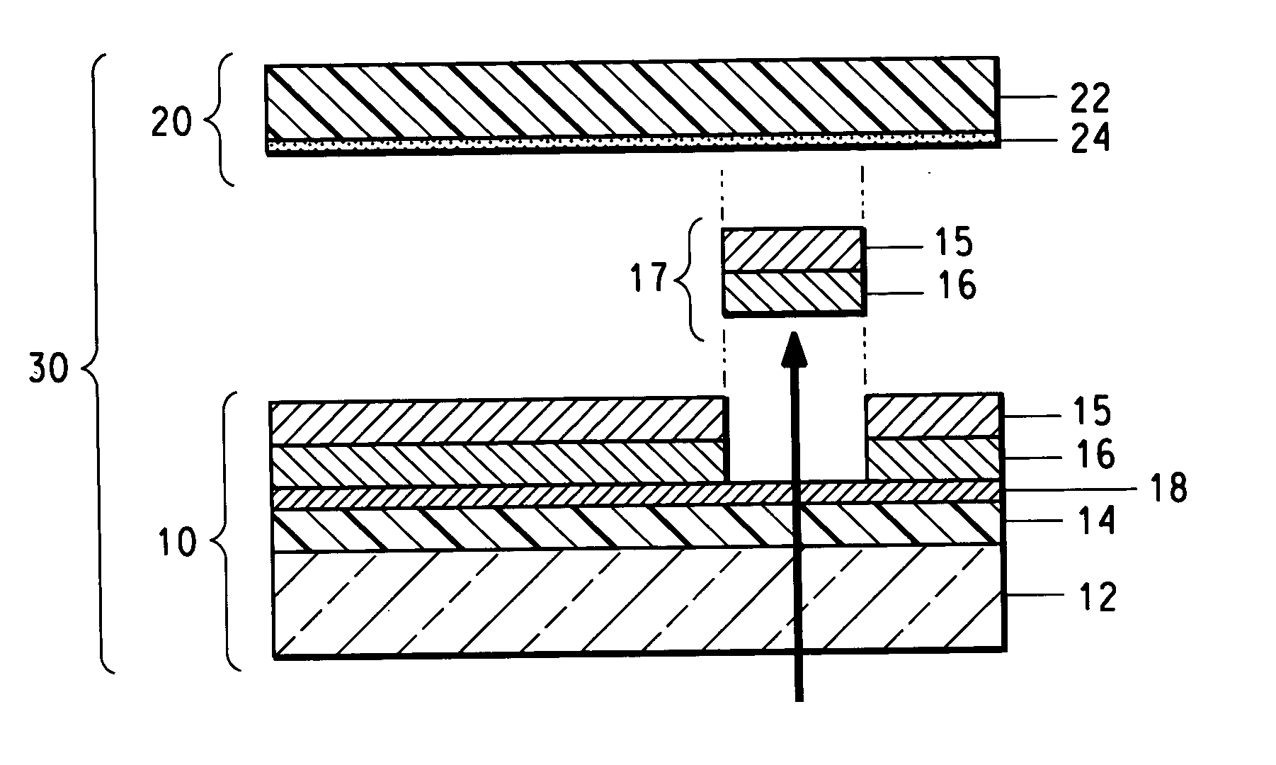
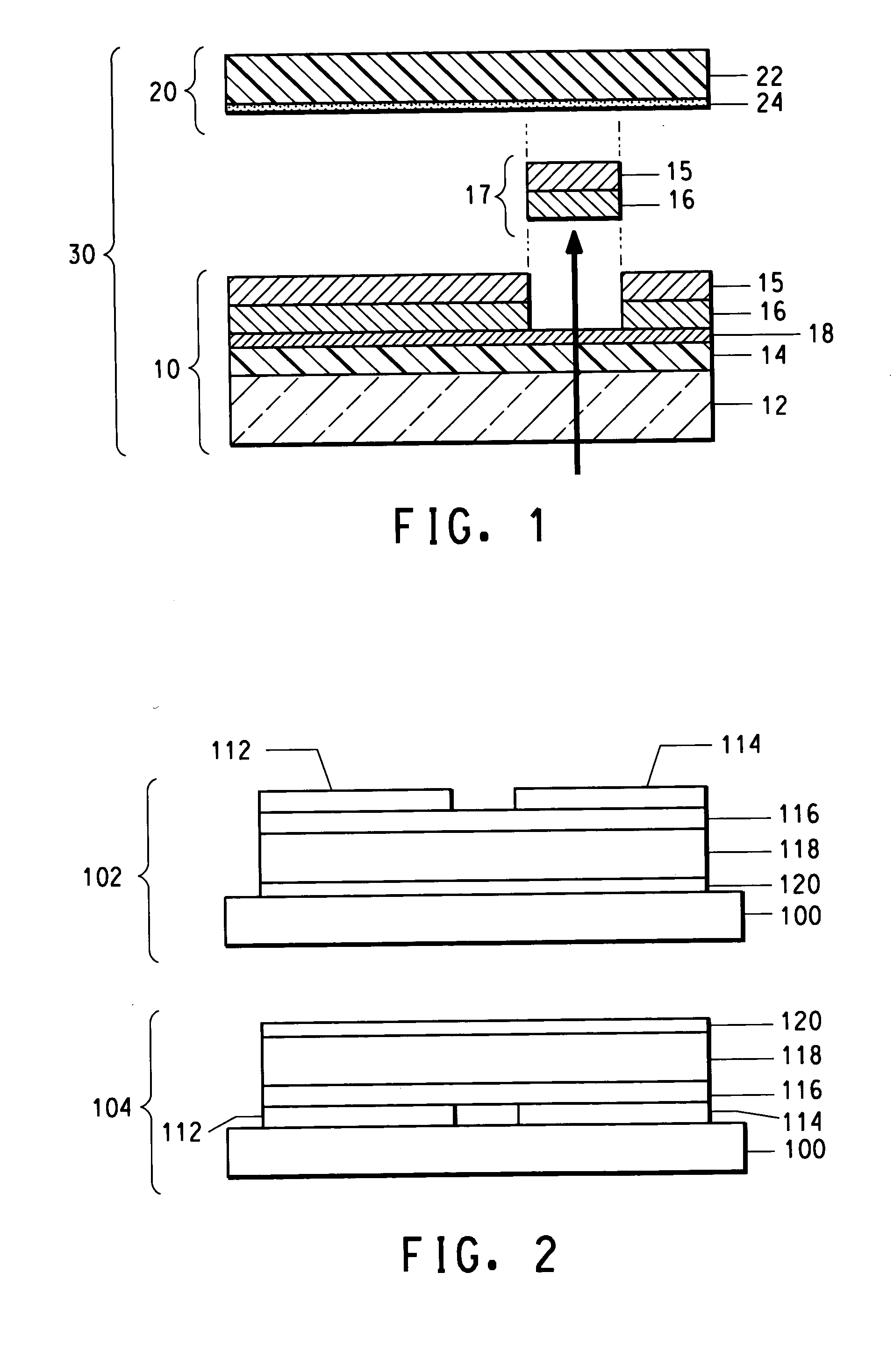
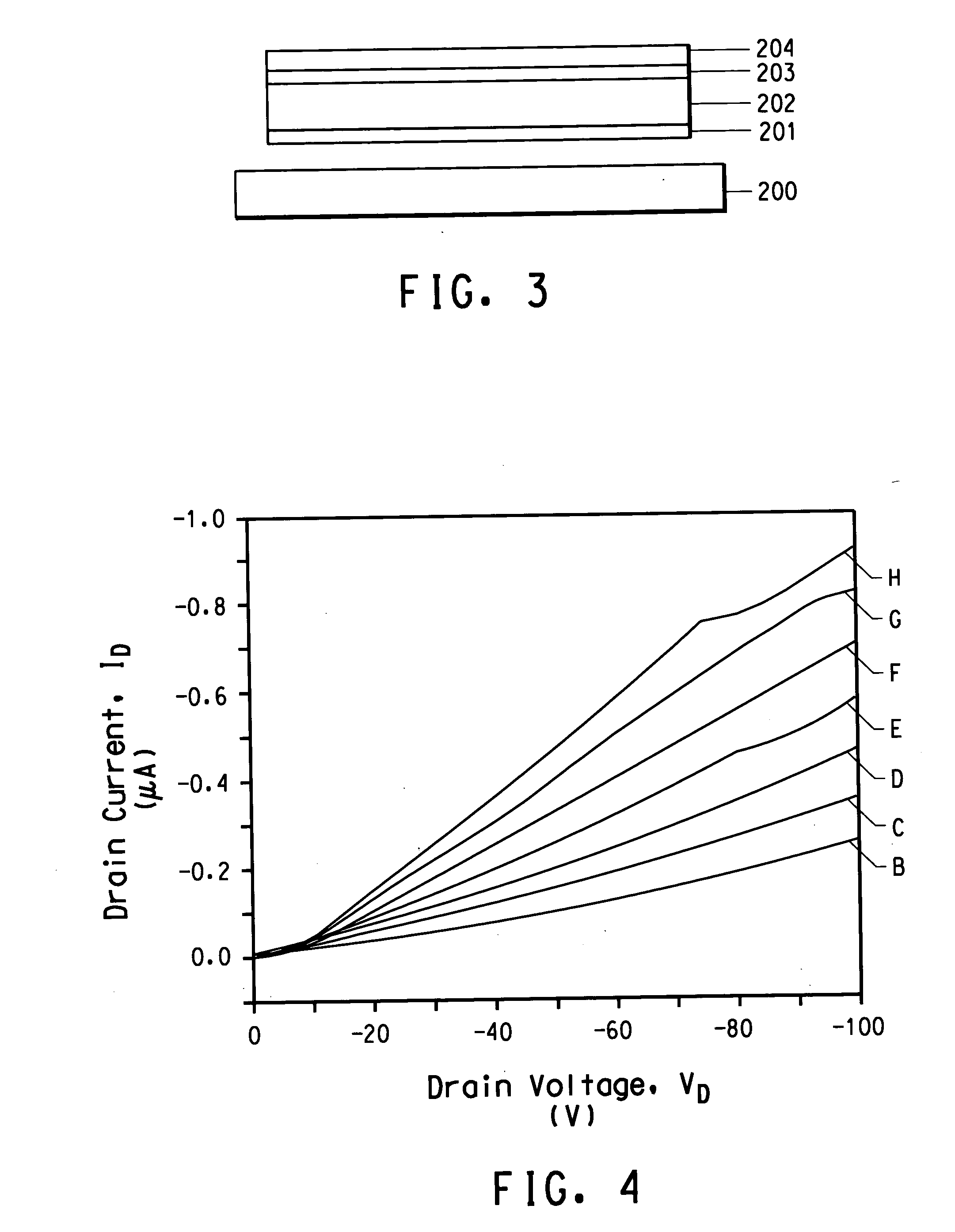
[0063] The TFT in bottom contact configuration described in the following example was printed via thermal imaging using four donor elements. Each of the donor elements included a 4 mil (0.0363 mm) thick substrate of Mylar®, 400 D optical clarity, available from E. I. DuPont de Nemours, Inc. (Wilmington, Del.) coated with 100 Å of nickel by electron beam deposition, to about 40% optical transmission.

[0064] The polyaniline (PANI) used was prepared through emulsion polymerization following the procedure outlined in U.S. Pat. No. 5,863,465. Dinonylnaphthalene sulfonic acid (DNNSA) was used as the dopant. The doped PANI is hereafter referred to as PANI-DNNSA. The addition of DNNSA was controlled such that the moles of sulfur atoms from the acid equaled the moles of nitrogen atoms in the backbone of the PANI. This was confirmed by elemental analysis after washing, separating and drying the resulting PANI-DNNSA. Carbon nanotubes were dispersed in PANI-DNNSA using an acoustic Dukane sonica...


PUM

PropertyMeasurementUnit
decomposition temperatureaaaaaaaaaa
thickaaaaaaaaaa
sizeaaaaaaaaaa

Abstract

Methods of forming a patterned semiconducting-dielectric material on a substrate by thermal processes are disclosed, comprising heating a thermally imageable donor element comprising a substrate and a transfer layer of semiconductive material in conjunction with a dielectric. The donor is exposed with the positive image of the desired pattern to be formed on the receiver, such that the exposed portions of the layer of semiconductive and dielectric material are simultaneously transferred, forming the desired pattern of semiconductive and dielectric material on the receiver. The semiconducting material can be patterned to form a thin film transistor. The method can also be used to pattern a light-emitting polymer or small molecule in conjunction with the charge injection layer to form the light-emitting display for light-sensitive organic electronic devices. Donor elements for use in the process are also disclosed. Methods for forming thin film transistors and donor elements for use in the processes, are also disclosed.

Description

FIELD OF THE INVENTION [0001] This invention relates to processes for transferring fragile or thermally sensitive materials by a thermal imaging process. This invention also relates to multi-layered structures useful in carrying out such processes. These processes include forming patterns of light-emitting polymers or semiconductive-dielectric material on substrates by laser-induced thermal transfer imaging. The invention relates to methods for forming thin film organic transistors (TFTs) and polymer light-emitting displays (PLEDs) by such thermal processes. TECHNICAL BACKGROUND OF THE INVENTION [0002] Thin film transistors have been fabricated incorporating organic semiconducting materials, such as pentacene, polythieneylenevinylene, thiophene oligomers, benzothiophene dimers, and polyacetylenes. Organic materials can also be used to form the other components of the transistor, such as the conducting layers that form the gate, source, and drain electrodes, and the insulating layers...

Claims


Application Information

Patent Timeline
Patent Type & Authority Applications(United States)
IPC IPC(8): B41M5/41B41M5/42B41M5/44B41M5/46G03C8/00H01L51/00H01L51/56
CPCB41M5/41B41M5/42B41M5/44B41M5/465B41M2205/06B41M2205/12B41M2205/30H01L51/0013H01L51/56H01L2251/5338Y10S430/146Y10S430/165B41M2205/38H10K71/18H10K2102/311H10K71/00
Inventor BLANCHET-FINCHER, GRACIELA BEATRIZ
Owner EI DU PONT DE NEMOURS & CO
Why Eureka
Try Eureka