

Semiconductor device and method for manufacturing the same
- Summary
- Abstract
- Description
- Claims
- Application Information
AI Technical Summary
Benefits of technology
Problems solved by technology
Method used
Image

Examples
first embodiment
Second Variation of First Embodiment
[0092]Hereinafter, a semiconductor device according to a second variation of the first embodiment of the present invention and a method for manufacturing the semiconductor device will be described with reference to the drawings.
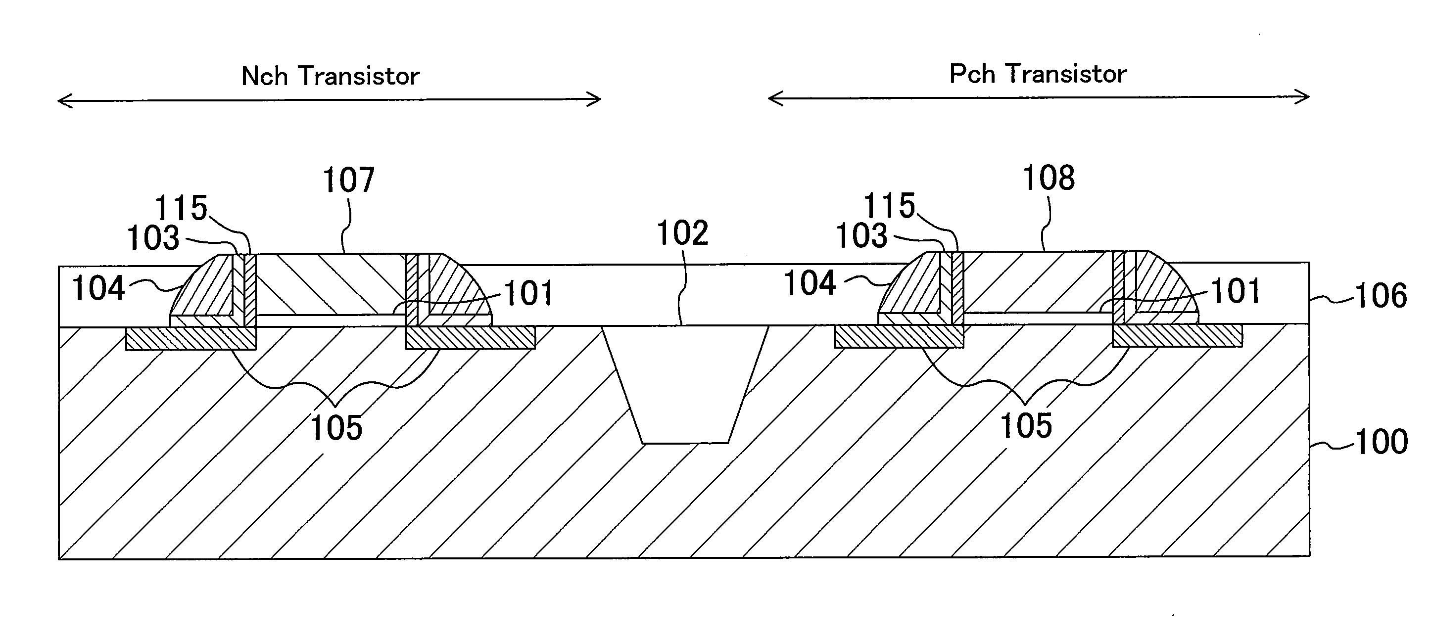
[0093]FIG. 15 is a cross-sectional view showing a structure of a gate electrode and its vicinity of the semiconductor device of the second variation of the first embodiment. Note that, in FIG. 15, the same parts as those of the first embodiment of FIG. 1 are indicated by the same reference numerals and will not be described.
[0094]As shown in FIG. 15, this variation is different from the first embodiment in that the height of the first gate electrode 107 in the Nch transistor is higher than the height of the second gate electrode 108 in the Pch transistor, and the heights of the offset spacers 115, the inner sidewall spacers 103, and the outer sidewall spacers 104 formed on the side surfaces of the first gate electrode 107 a...
second embodiment
Second Variation of Second Embodiment
[0125]Hereinafter, a semiconductor device according to a second variation of the second embodiment of the present invention and a method for manufacturing the semiconductor device will be described with reference to the drawings.
[0126]FIG. 29 is a cross-sectional view showing a structure of a gate electrode and its vicinity of the semiconductor device of the second variation of the second embodiment. Note that, in FIG. 29, the same parts as those of the second embodiment of FIG. 16 are indicated by the same reference numerals and will not be described.
[0127]As shown in FIG. 29, this variation is different from the second embodiment in that the height of the first gate electrode 207 in the Nch transistor is higher than the height of the second gate electrode 208 in the Pch transistor, and the heights of the offset spacers 215, the inner sidewall spacers 203, and the outer sidewall spacers 204 formed on the side surfaces of the first gate electrode...
PUM
 Abstract
Description
Claims
Application Information