Eureka AIR delivers breakthrough ideas for toughest innovation challenges, trusted by R&D personnel around the world.

Non-volatile memory device, non-volatile memory system and control method for the non-volatile memory device

a non-volatile memory and control method technology, applied in static storage, digital storage, instruments, etc., can solve the problems of increasing access time, increasing consumption current, increasing regulating time, etc., and achieves the effect of preventing the increase of consumption current, small and large load capacity of selector transistors

Active Publication Date: 2008-10-09
INFINEON TECH LLC
View PDF2 Cites 2 Cited by
  • Summary
  • Abstract
  • Description
  • Claims
  • Application Information

AI Technical Summary

Benefits of technology

The present invention provides a non-volatile memory device and system that can reduce consumption current and shorten access time during a burst operation. This is achieved by selectively accessing adjacent memory cells and applying a bias to the diffusion layer of a selected memory cell and the diffusion layer of at least one non-selected memory cell adjacent to the selected memory cell. The driving ability of a selector transistor is varied along the transition from one end to the other end of a memory block, which results in appropriate driving ability for both sequential and non-sequential access operations. This allows for efficient boosting of voltages on each occasion of accessing memory cells within a block, while preventing excessive boosting and speeding up burst accessing.

Problems solved by technology

Consequently, driving ability during the sequential access operation with less load capacity becomes redundant, leading to increase in consumption current.
Also, during a sequential access operation, excessively boosted voltage needs regulating into a predetermined voltage so that regulating time increases and hence access time increases.

Method used


Image

  • Non-volatile memory device, non-volatile memory system and control method for the non-volatile memory device
  • Non-volatile memory device, non-volatile memory system and control method for the non-volatile memory device
  • Non-volatile memory device, non-volatile memory system and control method for the non-volatile memory device

Examples


Embodiment Construction

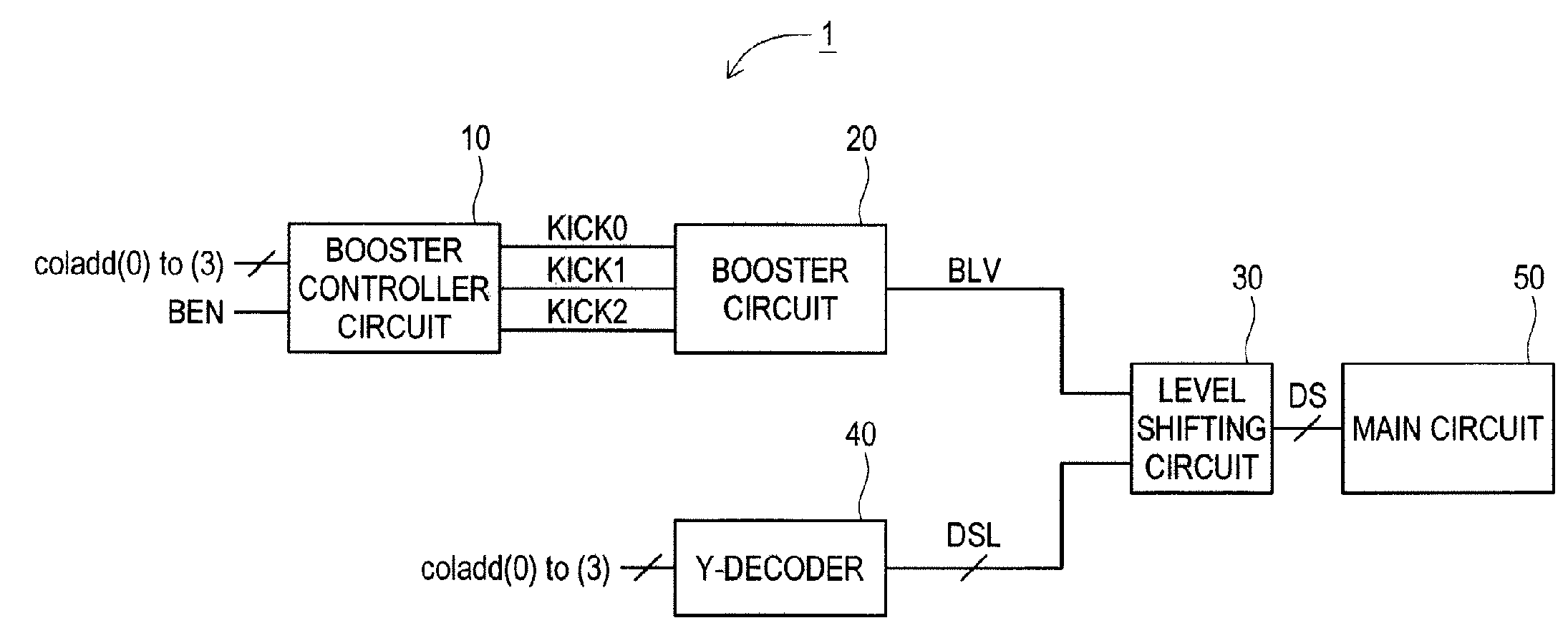
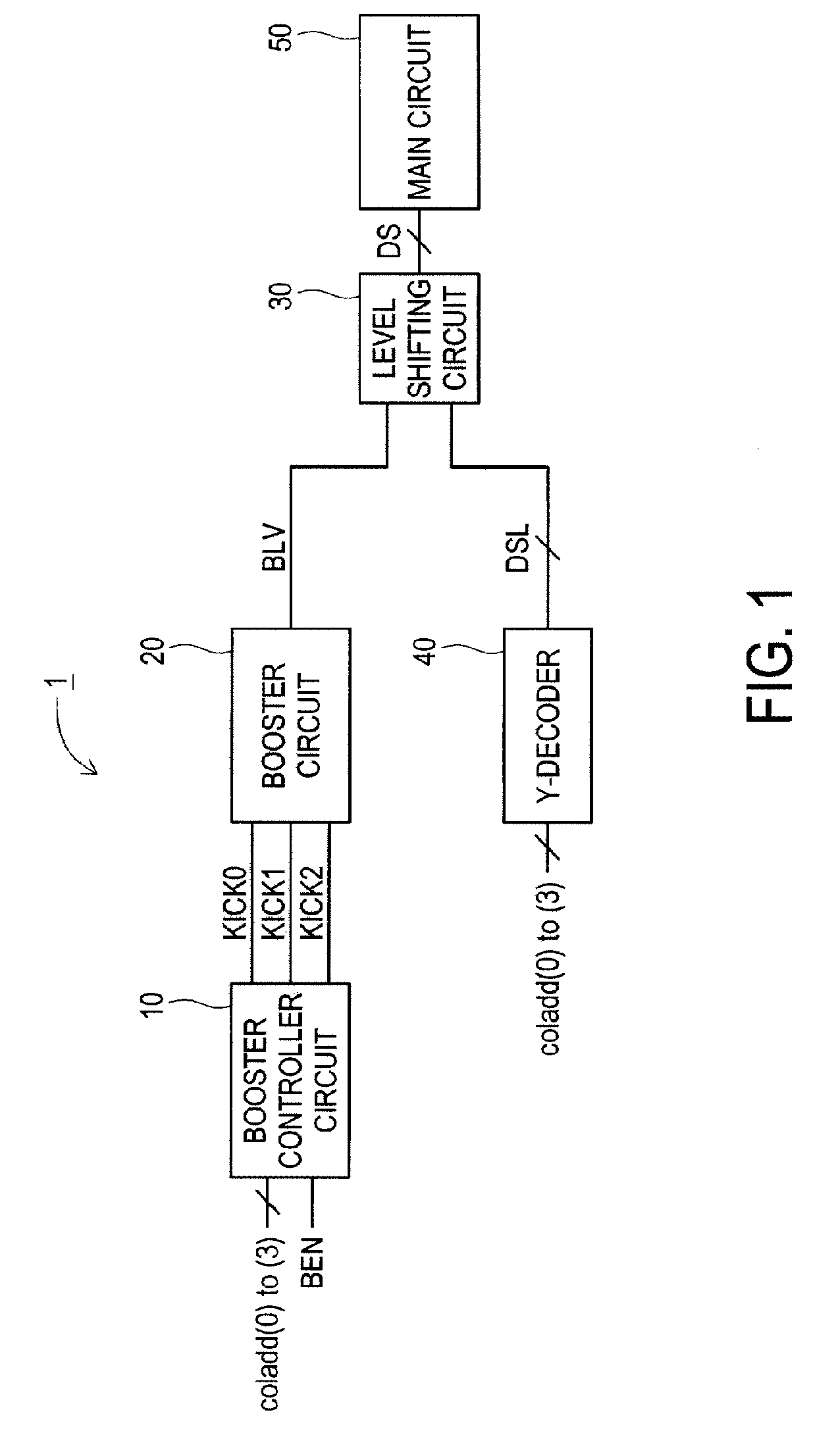
[0027]Referring now to FIGS. 1 to 9, a non-volatile memory device, non-volatile memory system and a non-volatile memory device control method of the invention will be hereinafter described in detail according to preferred embodiments. FIG. 1 shows an overall block diagram of a non-volatile memory device 1 of the invention. The non-volatile memory deice 1 comprises a booster controller circuit 10, a booster circuit 20, a level shifting circuit 30, a Y-decoder 40, and a main circuit 50.

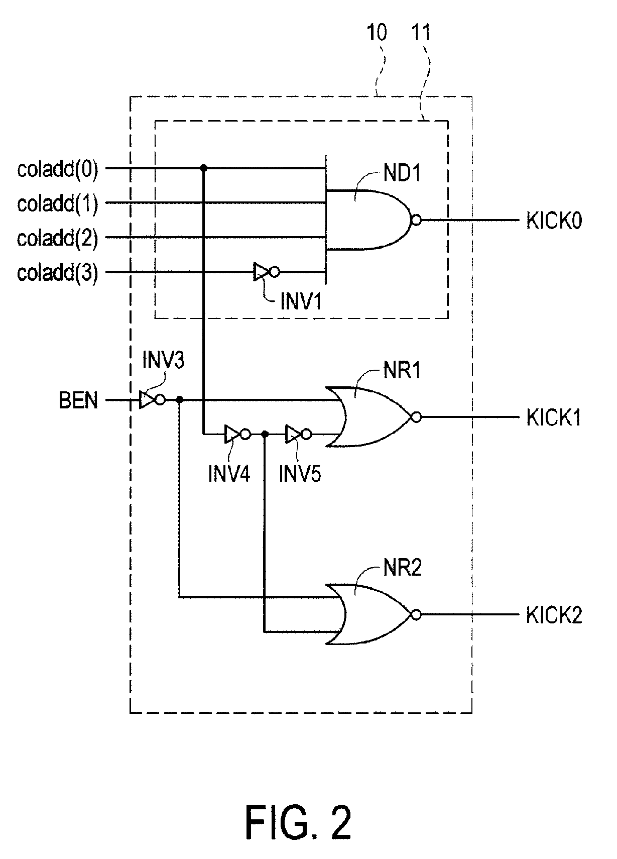
[0028]FIG. 2 shows a circuit diagram of the booster controller circuit 10. The booster controller circuit 10 comprises a KICK0 controller 11, NOR gates NR1 and NR2, inverters INV3 to INV5. To a NAND gate ND1 of the KICK0 controller 11, column addresses coladd(0) to (2) are inputted. Also to the NAND gate ND1, a column address coladd(3) is inputted through an inverter INV1. An output from the NAND gate ND1 is outputted as a kick signal KICK0.

[0029]To the NOR gate NR1, a boost enable signal BEN is inputte...


PUM


Abstract

A nonvolatile memory device which can reduce consumption current and shorten access time and a control method thereof is provided. The nonvolatile memory device 1 comprises a booster controller circuit 10, a booster circuit 20, a level-shifting circuit 30, a Y-decoder 40, and a main circuit 50. A NAND gate ND1, a NOR gate NR1, and a NOR gate NR2 provided in the booster controller circuit 10 output kick signals KICK0 to KICK2. The booster circuit 20 comprises boosting systems B0, B1, B2 which respectively receive the kick signals KICK0, KICK1, and KICK2. The kick signals KICK0 and KICK1 outputted from the NAND gate ND1 and the NOR gate NR1 make transition to high level in accordance with the transition of column address coladd from address 7 to 8. Therefore, the boosting system B0 is activated in addition to the boosting system B1.

Description

CROSS-REFERENCE TO RELATED APPLICATIONS[0001]The present invention is based on Japanese Patent Application No. 2007-097578 filed on Apr. 3, 2007, the entire disclosure of which is hereby incorporated by reference.TECHNICAL FIELD[0002]The invention relates to a nonvolatile memory device, non-volatile memory system and a control method for the non-volatile memory device. More particularly, the invention relates to the technique of reducing consumption current and shortening access time during an operation of reading out data from a memory cell having an insulating trap layer.BACKGROUND OF THE INVENTION[0003]In Published Japanese translation of PCT application No. 2005-537597, a flash memory device which employs the MirrorBit (registered trade mark) architecture is disclosed. In the MirrorBit architecture, two bits can be stored per memory cell. For reading out a memory cell, two column lines adjacent to the memory cell and auxiliary two column lines located outside of said two column ...

Claims


Application Information

Patent Timeline
Patent Type & Authority Applications(United States)
IPC IPC(8): G11C16/04G11C8/00G11C5/14
CPCG11C16/0491G11C16/26
Inventor KAWABATA, SHOZOPARK, SOOYONG
Owner INFINEON TECH LLC
Why Eureka
Eureka Blog
Learn More