Mold structure, imprinting method using the same, magnetic recording medium and production method thereof
a technology of magnetic recording medium and imprinting method, which is applied in the direction of photomechanical equipment, instruments, manufacturing tools, etc., can solve the problems of uniform output of data from the magnetic layer of the magnetic recording medium, the transfer quality of patterns is excellent, and the separability is superior
- Summary
- Abstract
- Description
- Claims
- Application Information
AI Technical Summary
Benefits of technology
Problems solved by technology
Method used
Image
Examples
first embodiment
>
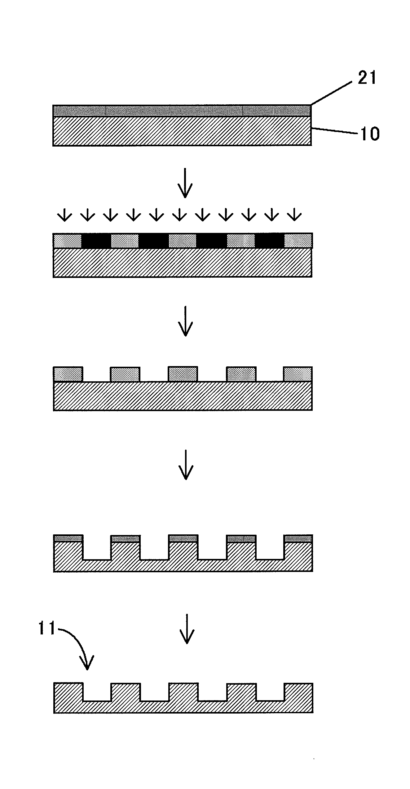
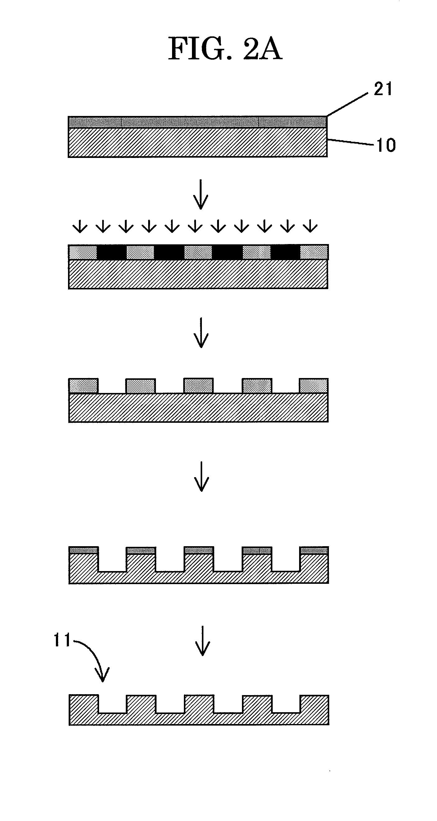
[0072]FIGS. 2A and 2B are cross-sectional views showing a method for producing a mold structure according to a first embodiment. First of all, as shown in FIG. 2A, a photoresist solution of PMMA, etc. is applied onto a Si substrate 10 by spin coating or the like to form a photoresist layer 21.
[0073]After that, while the Si substrate 10 is being rotated, a laser beam (or an electron beam) modulated correspondingly to a data recording track and a servo signal is applied onto the Si substrate 10, and the entire photoresist surface is exposed with predetermined patterns, for example a data track pattern formed of a pattern of convexities substantially in the shape of concentric circles, a servo pattern formed of a plurality of different patterns of convexities with different areas, and a buffer pattern formed of a pattern of convexities which are radially arranged and continuous in the radial direction between the data track pattern and the servo pattern.
[0074]Subsequently, the photore...
second embodiment
>
[0089]FIGS. 4A and 4B are process drawings showing a method for producing a mold structure according to a second embodiment. A master plate 11 having a concavo-convex pattern was produced as in the first embodiment.
>
[0090]A Ni mold structure was produced by forming a conductive film on the surface of the master plate by sputtering, and immersing the master plate provided with the conductive film in a Ni electroforming bath to electroform the master plate.
[0091]A conductive film 22 can be formed on the concavo-convex pattern of the master plate 11 by processing a conductive material in accordance with a vacuum deposition method such as vacuum vapor deposition, sputtering or ion plating, a plating method, or the like. The conductive material can be suitably selected according to a subsequent step (electroforming), but it is preferably a Ni-based, Fe-based or Co-based metal / alloy material or the like. It is desirable that the thickness of the Ni mold structure obtained through the ele...
third embodiment
>
[0093]FIGS. 5A and 5B are process drawings showing a method for producing a mold structure according to a third embodiment. A master plate 11 having a concavo-convex pattern was produced as in the first embodiment.
>
[0094]The master plate 11 was pressed against a thermoplastic resin sheet 31. After that, by heating the sheet to a temperature equal to or higher than the softening temperature of the resin, the viscosity of the resin decreased, and the pattern of convex portions formed on the master plate was transferred onto the resin sheet 31. Subsequently, the transferred pattern was cured by cooling, and the resin sheet was peeled away from the master plate 11 to yield a resin mold structure 1 having a concavo-convex shape.
[0095]Here, the resin material is not particularly limited and can be suitably selected according to the purpose, as long as it has thermoplasticity, transmits light and has the strength necessary for it to function as a mold structure. Examples thereof include P...
PUM
| Property | Measurement | Unit |
|---|---|---|
| thickness | aaaaa | aaaaa |
| average roughness Rz2 | aaaaa | aaaaa |
| average roughness Rz1 | aaaaa | aaaaa |
Abstract
Description
Claims
Application Information


