Conductive dome probes for measuring system level multi-ghz signals

a technology of conductive dome probes and multi-ghz signals, which is applied in the direction of high-frequency circuit adaptations, instruments, final product manufacturing, etc., can solve the problems of increasing the number of input/output (i/o) pins, configuration pins, other types of pins of ics required for power and interface with other components, and increasing the complexity of processing applications

Active Publication Date: 2008-10-09
CISCO TECH INC
View PDF8 Cites 49 Cited by
  • Summary
  • Abstract
  • Description
  • Claims
  • Application Information

AI Technical Summary

Problems solved by technology

As processing applications become increasingly more complex, the number of input / output (I / O) pins, configuration pins, and other types of pins of ICs required for power and to interface with other components continues to grow.
Corresponding reductions in package size present a challenge to package designers faced with accommodating the increased pin count.
However, properly connecting a high density BGA ASIC to a PCB to route signals and maintain signal integrity creates numerous problems for both the ASIC designers and the printed circuit board designers.

Method used


Image

  • Conductive dome probes for measuring system level multi-ghz signals
  • Conductive dome probes for measuring system level multi-ghz signals
  • Conductive dome probes for measuring system level multi-ghz signals

Examples


Embodiment Construction

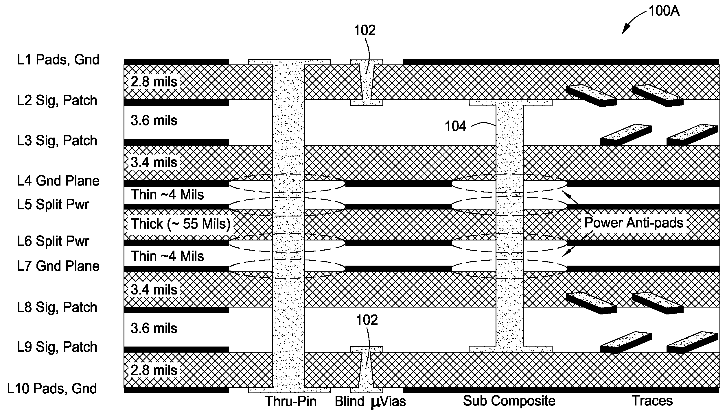
[0038]Embodiments of the present invention provide techniques for optimizing application specific integrated circuit (ASIC) and other IC pin assignment corresponding to a high density interconnect (HDI) printed circuit board (PCB) layout. Applying the techniques described herein, pin assignments may be systematically and strategically planned, for example, in an effort to reduce the PCB layer count and associated cost, increase signal integrity and speed, reduce the surface area used by an ASIC and its support circuitry, reduce plane perforations, and reduce via crosstalk over conventional designs with an ASIC mounted on a multilayered PCB.

[0039]Many of the techniques described herein may be applied to any integrated circuit (IC). To facilitate understanding and since board developers interested in these techniques may have the most control over custom ASIC pin assignments, the techniques are described in relation to ASICs as a specific example.

[0040]PCBs with multiple layers are ty...


PUM


Abstract

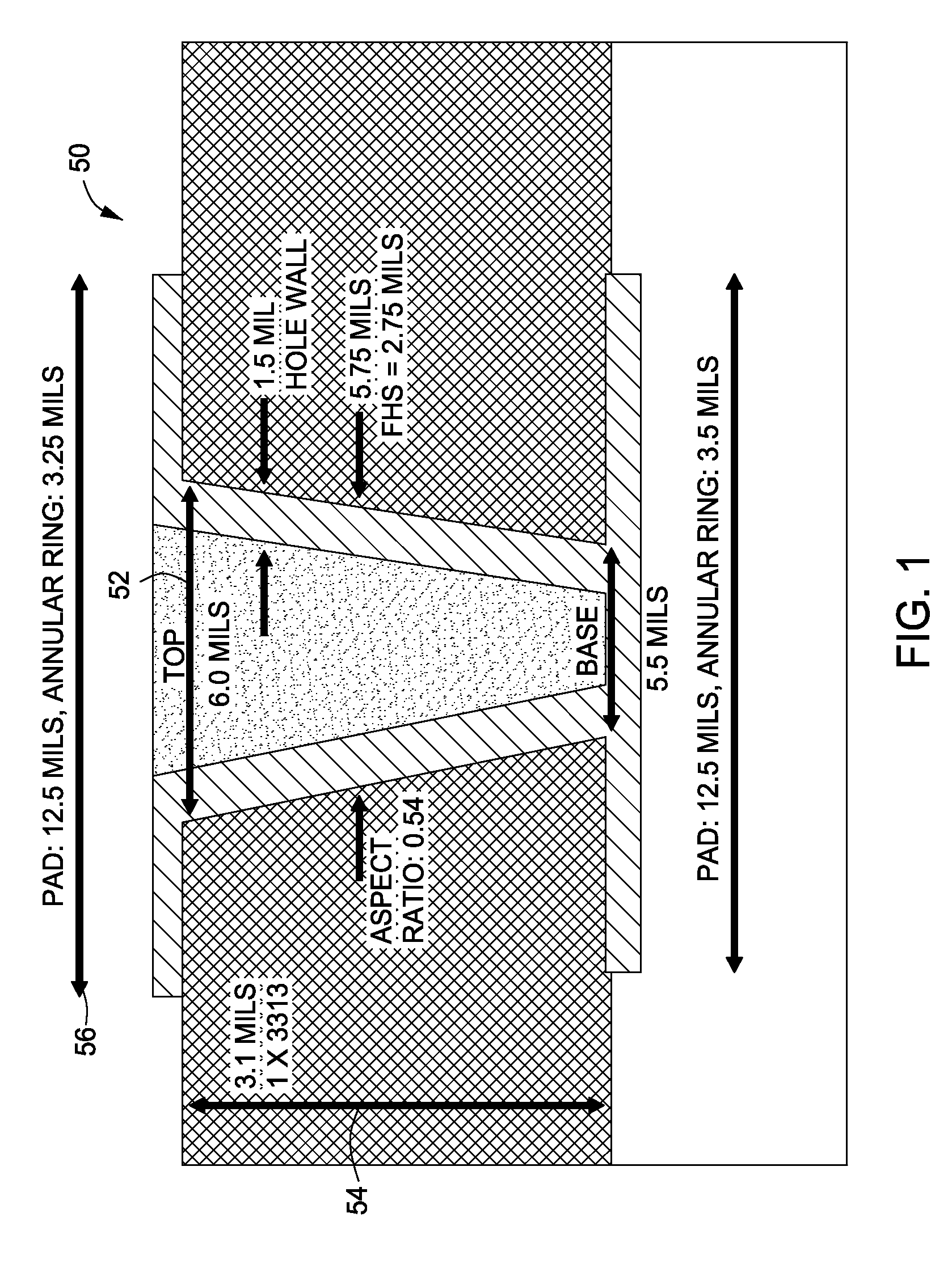
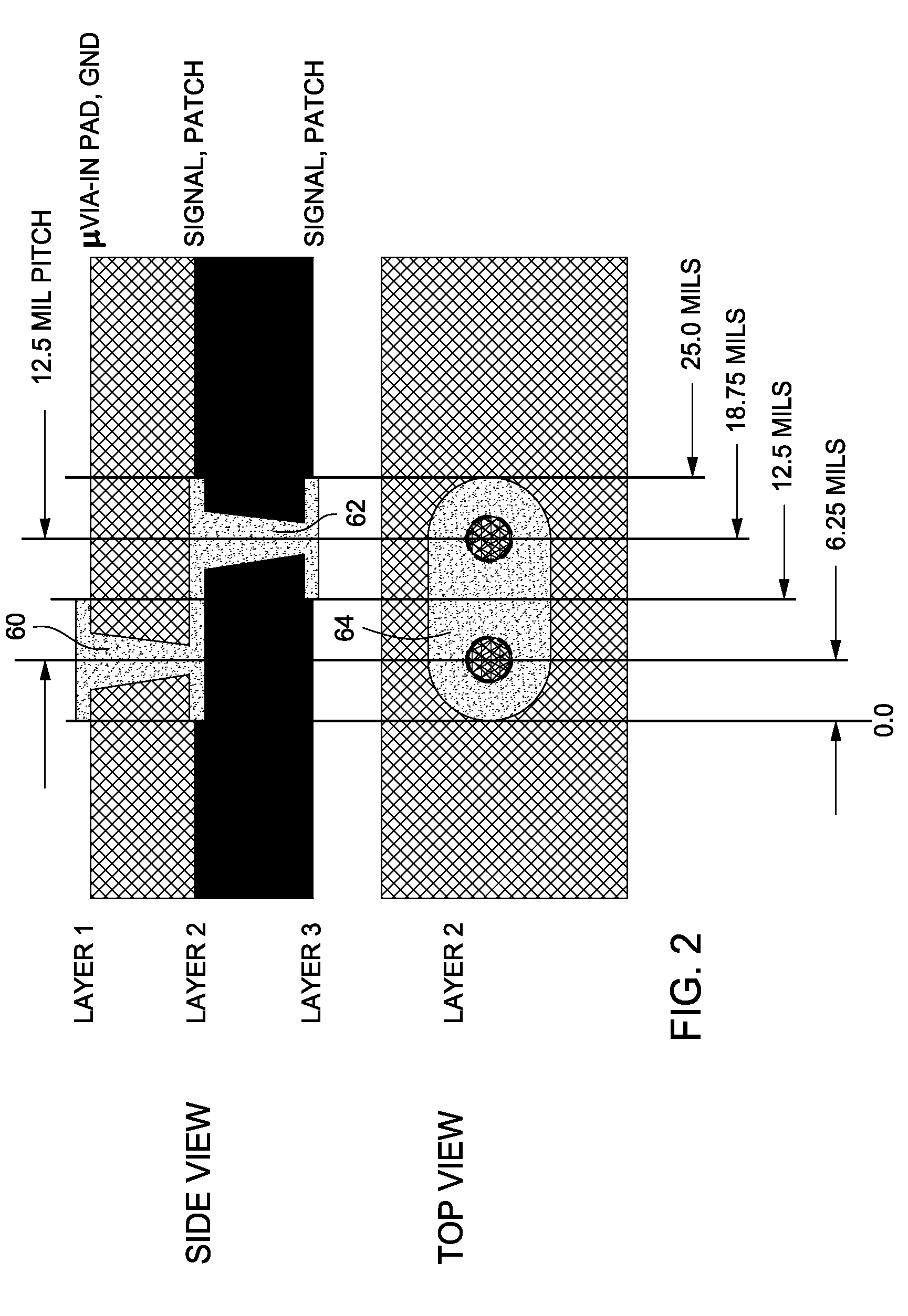
Methods and apparatus for accessing a high speed signal routed on a conductive trace on an internal layer of a printed circuit board (PCB) using high density interconnect (HDI technology) are provided. The conductive trace may be coupled to a microvia (μVia) having a conductive dome disposed above the outer layer pad of the μVia. In-circuit test (ICT) fixtures or high speed test probes may interface with the conductive dome to test the high speed signal with decreased reflection loss and other parasitic effects when compared to conventional test points utilizing plated through-hole (PTH) technology.

Description

BACKGROUND OF THE INVENTION[0001]1. Field of the Invention[0002]Embodiments of the present invention generally relate to integrated circuits (ICs) and multilayer printed circuit boards (PCBs).[0003]2. Description of the Related Art[0004]As processing applications become increasingly more complex, the number of input / output (I / O) pins, configuration pins, and other types of pins of ICs required for power and to interface with other components continues to grow. It is not uncommon for some application-specific ICs (ASICs) to possess pin counts that exceed 2000. Advancements in technology continually push the envelope to design smaller and smaller surface mount ASICs. Corresponding reductions in package size present a challenge to package designers faced with accommodating the increased pin count.[0005]One approach to meeting the packaging requirements has been to encapsulate ASICs in a surface-mountable ball grid array (BGA). Using a grid of solder balls as its connectors, a BGA enabl...

Claims


Application Information

Patent Timeline
Patent Type & Authority Applications(United States)
IPC IPC(8): G06F17/50G01R31/00
CPCH05K2201/10484H05K1/0262H05K2201/10734G01R31/2818H05K1/0231H05K1/0237H05K1/0268H05K1/113H05K1/181H05K3/3421H05K3/3457H05K3/429H05K3/4602H05K3/4623H05K2201/0367H05K2201/09227H05K2201/09236H05K2201/093H05K2201/09309H05K2201/09536H05K2201/09627H05K2201/09663H05K2201/10333H05K2201/10462H05K2201/10545Y02P70/50
Inventor BIRD, STEVEN C.MALIAN, VAROUJANAHMAD, MUDASIRCASALE, CHARLES H.TANG, DANLU
Owner CISCO TECH INC
Why Eureka
Try Eureka