Image sensor and method of fabrication

a technology of image sensor and fabrication method, which is applied in the field of image sensor, can solve the problems of losing the effective throughput of the desired incident light, and achieve the effect of reducing the optical loss of incident light and increasing the quantity

Inactive Publication Date: 2008-10-16
SAMSUNG ELECTRONICS CO LTD
View PDF9 Cites 57 Cited by
  • Summary
  • Abstract
  • Description
  • Claims
  • Application Information

AI Technical Summary

Benefits of technology

[0012]Accordingly, embodiments of the invention are directed to an image sensor adapted to reduce the optical loss of incident light in relation to photoelectric transformation regions of the image sensor. Stated in positive terms, embodiments of the invention are directed to an image sensor adapted to increase the quantity (e.g., the intensity) of incident light received by photoelectric transformation regions of the image sensor. Embodiments of the invention are also directed to related methods of fabricating such an image sensor.
[0013]In one embodiment of the invention, an image sensor is provided with a reduced number of interlayer insulation films associated with color filter layers and photoelectric transformation regions.

Problems solved by technology

Such undesired light acts a noise signal to the intended incident light.
This optical interference causes a loss the effective throughput of the desired incident light.

Method used


Image

  • Image sensor and method of fabrication
  • Image sensor and method of fabrication
  • Image sensor and method of fabrication

Examples


Embodiment Construction

[0026]Several embodiments of the invention will be described below in some additional detail with reference to the accompanying drawings. The present invention may, however, be embodied in different forms and should not be constructed as being limited to only the embodiments set forth herein. Rather, these embodiments are presented as teaching examples. It will also be understood from the following description that when a layer (or film), or element is referred to as being “on” another layer (or film), element, or substrate, it may be “directly on” the other layer (or film), element, or substrate, or intervening layers (or films) or elements may also be present.

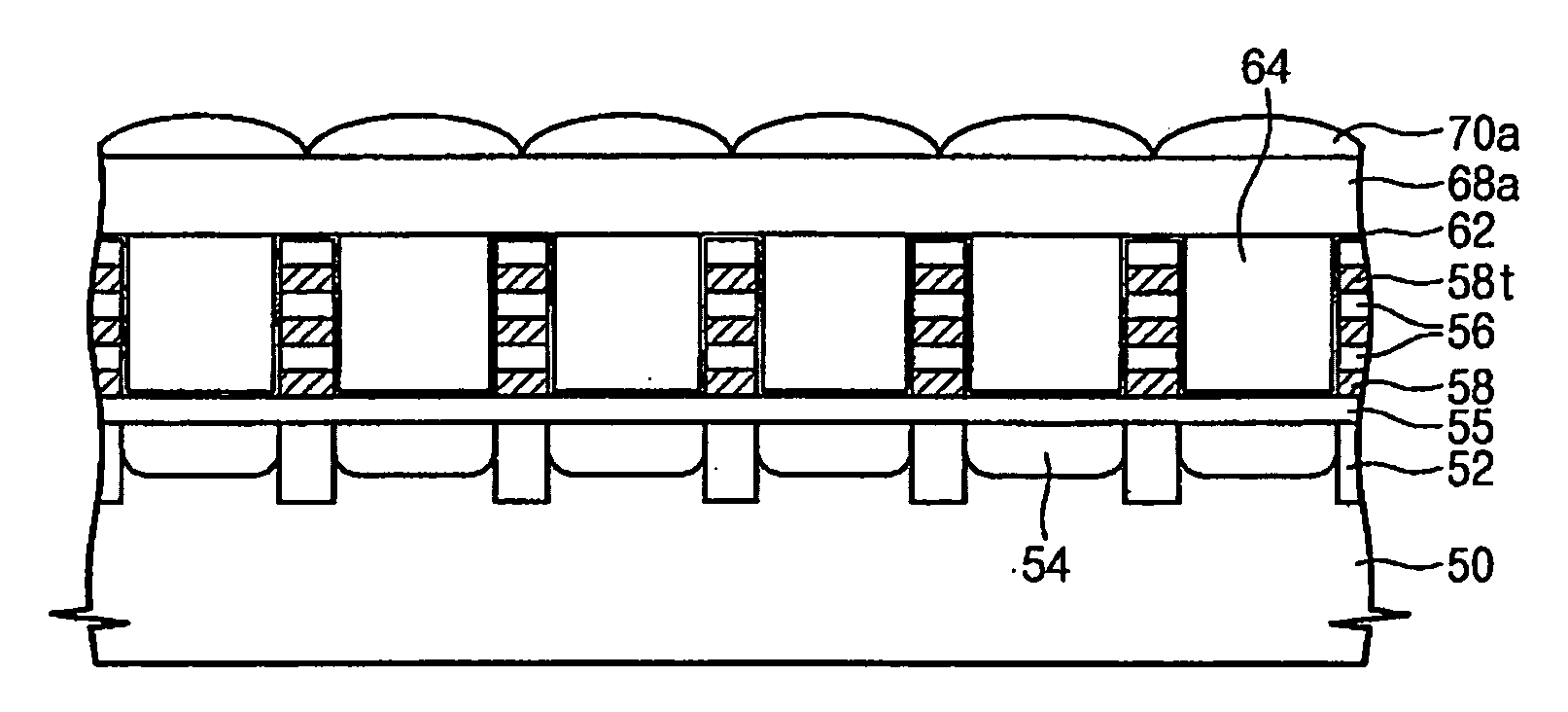
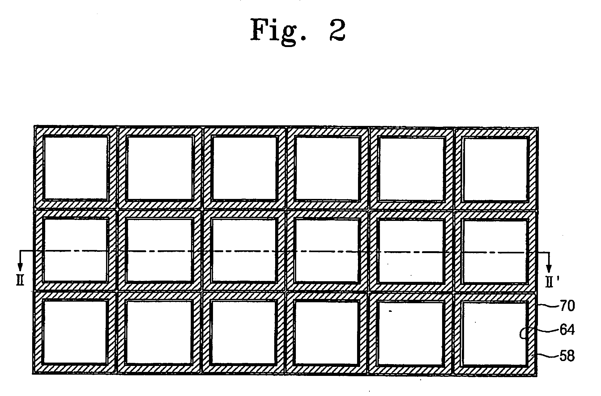
[0027]FIG. 2 is a plane view illustrating an image sensor in accordance with a first embodiment of the invention. FIG. 3A is a related sectional view taken along with the line II-II′ of FIG. 2.

[0028]With reference to FIGS. 2 and 3A, field isolation regions 52 are formed in a semiconductor substrate 50 to define pixel regions ...


PUM


Abstract

Disclosed is an image sensor and method of fabricating the same. The image sensor includes a photoelectric transformation region formed in a semiconductor substrate, and pluralities of interlayer dielectric films formed over the photoelectric transformation regions. The interlayer dielectric films contain multilevel interconnection layers. A color filter layer is disposed in a well region formed in the interlayer dielectric films over the photoelectric transformation region. A passivation layer is interposed between the color filter layer and the interlayer dielectric films.

Description

CROSS REFERENCE TO RELATED APPLICATION[0001]This is a divisional of U.S. application Ser. No. 11 / 336,906, filed Jan. 23, 2006, which is incorporated herein by reference in its entirety.BACKGROUND OF THE INVENTION[0002]1. Field of the Invention[0003]Embodiments of the invention relate to image sensors. More particularly, embodiments of the invention relate to an image sensor having improved optical sensitivity and a related method of fabrication.[0004]2. Discussion of Background Art[0005]Image sensors convert incident light into corresponding electrical signals (e.g., digital data) which may subsequently be used to form still or moving images. The term “incident light” generally refers to optical energy of any reasonable wavelength received by an image sensor. Conventional image sensors are basically composed of a pixel array. The pixel array is formed in turn by a uniform arrangement of photoelectric transformation regions, such as photodiodes. In order to detect, process, and outpu...

Claims


Application Information

Patent Timeline
Patent Type & Authority Applications(United States)
IPC IPC(8): H01L27/00
CPCH01L27/14621H01L27/14627H01L27/14685H01L31/02161H01L31/02162H01L27/146
Inventor PARK, YOUNG-HOONOH, TAE-SEOKKIM, EUN-SOOLEE, JUNE-TAEG
Owner SAMSUNG ELECTRONICS CO LTD
Why Eureka
Try Eureka