Semiconductor integrated circuit

Active Publication Date: 2008-10-16
SOCIONEXT INC
View PDF9 Cites 17 Cited by
  • Summary
  • Abstract
  • Description
  • Claims
  • Application Information

AI Technical Summary

Benefits of technology

[0016]An object of the present invention is to provide a semiconductor integrated circuit having memory cells, in which a static noise margin can be improved irrespective of variations in transistor characteristics or variations in an operating environment.
[0018]Thus, since the pull-down transistor for pulling down a word line is provided, the voltage of the word line in the active state can be suppressed, so that the static noise margin of the memory cell can be improved. The pull-down transistor has the same conductivity type as that of the transistor for causing the word line to go into the active state, so that the voltage of the word line in the active state can be optimally controlled irrespective of variations in transistor characteristics or a change in an operating environment, such as a power supply voltage, temperature or the like.
[0019]According to the present invention, the voltage of a word line in the active state can be optimized. Since the static noise margin of a memory cell can be improved, a semiconductor integrated circuit having stable memory cell characteristics and low power consumption can be achieved.

Problems solved by technology

This leads to detrimental effects.
For example, in a semiconductor integrated circuit having flip-flop memory cells, such as a static random access memory (hereinafter referred to as an SRAM), it has been considerably difficult to impart stable characteristics to the memory cells due to variations in characteristics of transistors included in the memory cells or the reduction of the power supply voltage.
However, if two different power supply voltages cannot be supplied to an SRAM (only one power supply voltage is supplied), a method as described in Patent Document 1 cannot be used.
Also, if a step-up power supply circuit or a step-down power supply circuit is provided as in Patent Document 1, a power supply for the whole peripheral circuit or the whole memory array is controlled, resulting in an increase in power consumption.
Also, the transfer gate is connected in series to a word driver circuit for driving the word line, and therefore, the capability to drive the word line is reduced, leading to a deterioration in the rising or falling speed of the word line voltage.
Further, if the word line is caused to be in the active state for a long period of time, the word line voltage goes up to the power supply voltage level due to a leakage current via the transfer gate or the like.
The influence of variations in elements constituting the circuit is not taken into consideration, and therefore, when the reduced process rule is used, it is considerably difficult to achieve the stable characteristics and performance of the semiconductor integrated circuit.

Method used


Image

  • Semiconductor integrated circuit
  • Semiconductor integrated circuit
  • Semiconductor integrated circuit

Examples


first embodiment

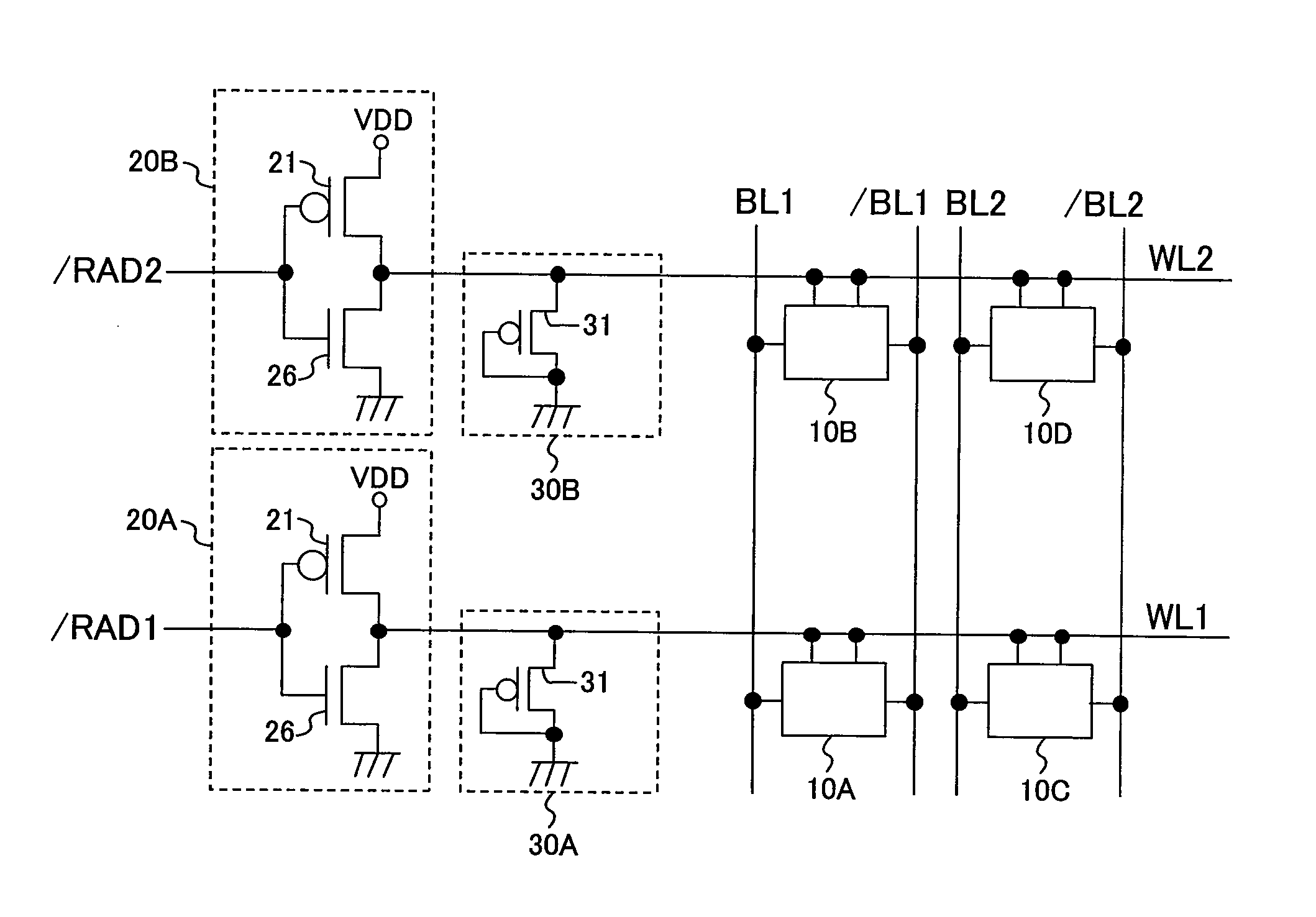
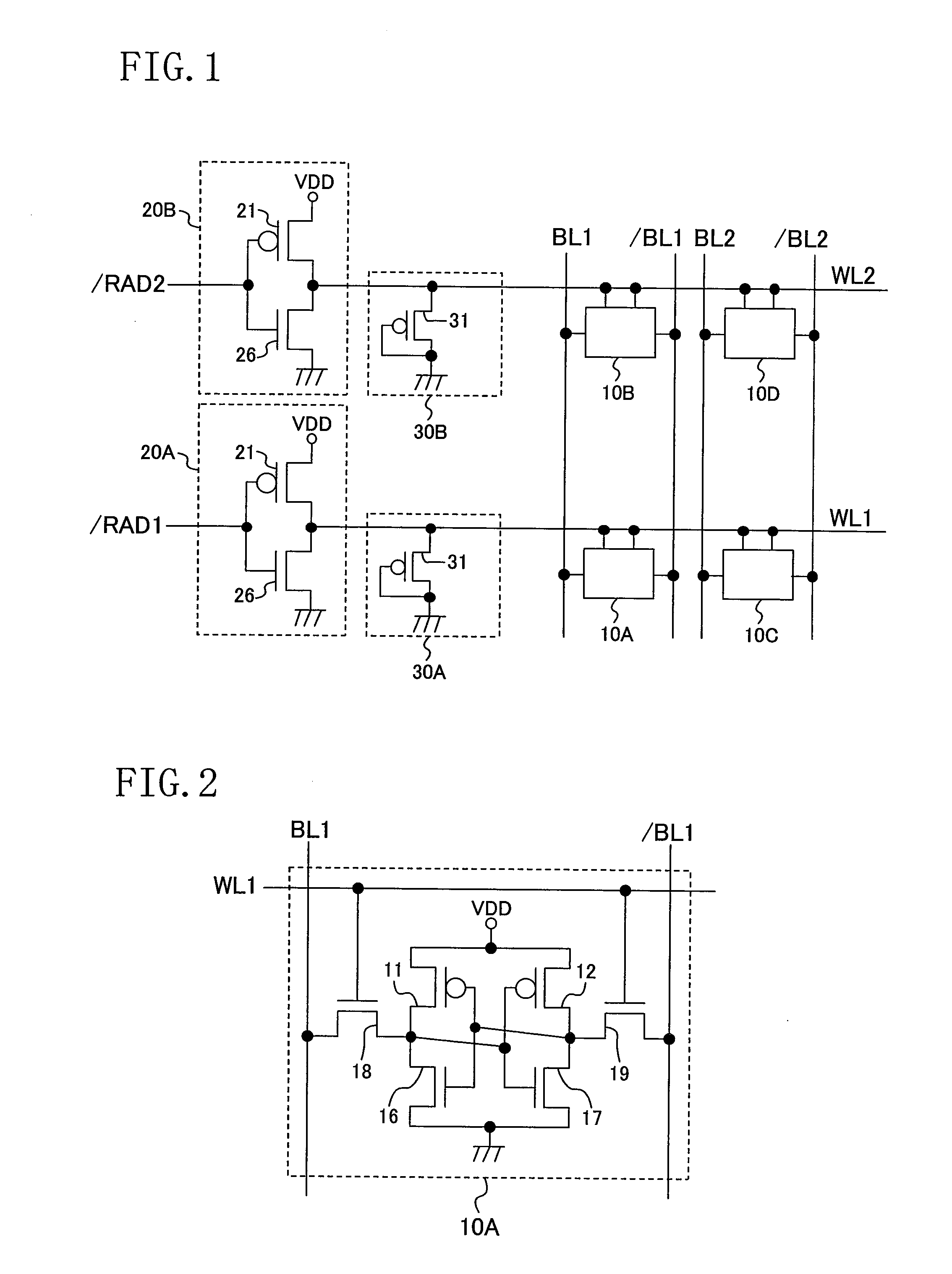
[0030]FIG. 1 is a block diagram showing a configuration of a semiconductor integrated circuit according to a first embodiment of the present invention. The semiconductor integrated circuit of FIG. 1 has memory cells 10A, 10B, 10C and 10D, word line drivers 20A and 20B, and pull-down circuits 30A and 30B.

[0031]The word line drivers 20A and 20B each have a PMOS transistor 21 and an NMOS transistor 26. The pull-down circuits 30A and 30B each have a PMOS transistor 31 as a pull-down transistor.

[0032]In the word line drivers 20A and 20B, the PMOS transistor 21 and the NMOS transistor 26 constitute an inverter. The word line drivers 20A and 20B invert row address signals / RAD1 and / RAD2 and output the results to the word lines WL1 and WL2, respectively.

[0033]In the pull-down circuits 30A and 30B, the source terminals of the PMOS transistors 31 are connected to the word lines WL1 and WL2, respectively. The gate terminal and the drain terminal of the PMOS transistor 31 are both connected to...

second embodiment

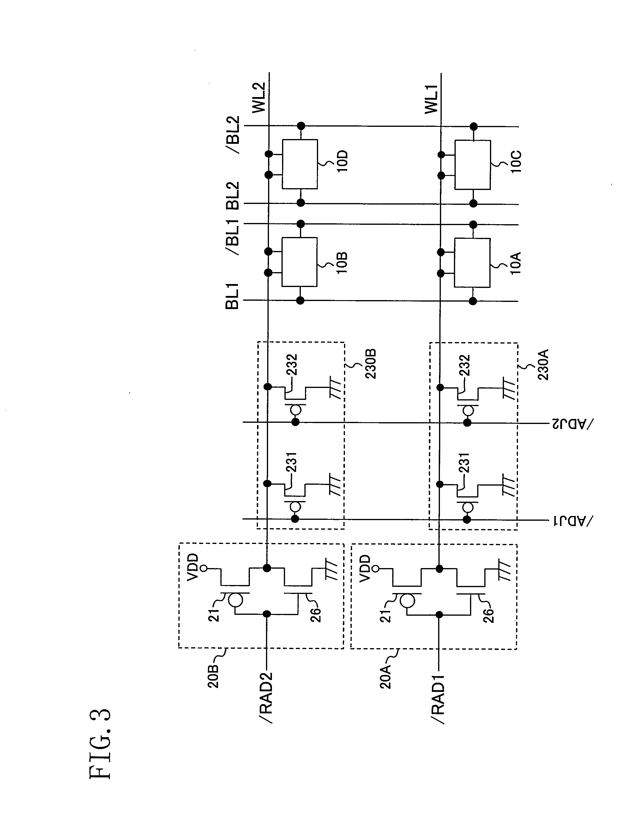
[0050]FIG. 3 is a block diagram showing a configuration of a semiconductor integrated circuit according to a second embodiment of the present invention. The semiconductor integrated circuit of FIG. 3 is similar to the semiconductor integrated circuit of FIG. 1, except that pull-down circuits 230A and 230B are provided instead of the pull-down circuits 30A and 30B. The other parts are indicated by the same reference symbols and will not be described.

[0051]The pull-down circuit 230A has PMOS transistors 231 and 232 as pull-down transistors. In the pull-down circuit 230A, the source terminals of the PMOS transistors 231 and 232 are connected to the word line WL1, and the drain terminals thereof are connected to the ground. Word line voltage adjustment signals / ADJ1 and / ADJ2 are given to the gate terminals of the PMOS transistors 231 and 232, respectively. The pull-down circuit 230B is similar to the pull-down circuit 230A, except that the pull-down circuit 230B is connected to the wor...

third embodiment

[0063]FIG. 4 is a block diagram showing a configuration of a semiconductor integrated circuit according to a third embodiment of the present invention. The semiconductor integrated circuit of FIG. 4 is similar to the semiconductor integrated circuit of FIG. 1, except that pull-down circuits 330A and 330B are provided instead of the pull-down circuits 30A and 30B and a pull-down control circuit 40 is further provided. The other parts are indicated by the same reference symbols and will not be described.

[0064]The pull-down circuits 330A and 330B each have a PMOS transistor 331 as a pull-down transistor. In the pull-down circuits 330A and 330B, the source terminals of the PMOS transistors 331 are connected to the word lines WL1 and WL2, respectively. A pull-down control signal / PD is given to the gate terminal of the PMOS transistor 331, and the drain terminal thereof is connected to the ground.

[0065]The pull-down control circuit 40 has PMOS transistors 41 and 42. The PMOS transistors ...


PUM


Abstract

A semiconductor integrated circuit includes a plurality of memory cells arranged in a matrix, a plurality of word lines corresponding to respective rows of the plurality of memory cells, a plurality of word line drivers for driving the plurality of word lines, respectively, and a plurality of pull-down circuits connected to the plurality of word lines, respectively, for causing voltages of the respective connected word lines to be lower than or equal to a power supply voltage when the respective word lines are in an active state. The word line drivers each have a transistor for causing the corresponding word line to go into the active state. The pull-down circuits each have a pull-down transistor for pulling down the corresponding word line, the pull-down transistor being a transistor having the same conductivity type as that of the transistor included the word line driver for driving the corresponding word line.

Description

CROSS REFERENCE TO RELATED APPLICATIONS[0001]This Non-provisional application claims priority under 35 U.S.C. §119(a) on Patent Application No. 2007-104823 filed in Japan on Apr. 12, 2007, the entire contents of which are hereby incorporated by reference.BACKGROUND OF THE INVENTION[0002]1. Field of the Invention[0003]The present invention relates to a semiconductor integrated circuit having flip-flop memory cells and, more particularly, to a technique of controlling the voltage of a word line.[0004]2. Description of the Related Art[0005]In recent years, as the process rule is reduced, the areas and the power supply voltages of semiconductor integrated circuits are rapidly reduced. This leads to detrimental effects. For example, in a semiconductor integrated circuit having flip-flop memory cells, such as a static random access memory (hereinafter referred to as an SRAM), it has been considerably difficult to impart stable characteristics to the memory cells due to variations in chara...

Claims


Application Information

Patent Timeline
IPC IPC(8): G11C11/00G11C8/08
CPCG11C8/08G11C11/412G11C11/413G11C29/02G11C29/021G11C29/028G11C29/48G11C2029/5002G11C2029/5004G11C2029/5006
Inventor YAMAGAMI, YOSHINOBU
Owner SOCIONEXT INC
Why Eureka
Try Eureka