
Method for Accelerated Etching of Silicon

Inactive Publication Date: 2008-10-16
ROBERT BOSCH GMBH
View PDF37 Cites 178 Cited by
  • Summary
  • Abstract
  • Description
  • Claims
  • Application Information

AI Technical Summary

Benefits of technology

[0006]The etching method according to example embodiments of the present invention and its use have the advantage that very rapid etching of silicon without plasma is made possible. Even great etching depths may thus be achieved in an accelerated manner and the required etching time may therefore be significantly shortened. The method reduces the manufacturing costs for chips having pronounced depth structuring in this manner.

Problems solved by technology

However, it is fundamentally different in principle that the manufacture of an electronic circuit typically represents a planar problem, while micromechanical components typically are three-dimensional, i.e., the structuring depth is unequally pronounced.
However, refining this technology for etching silicon is neither discussed nor suggested.

Method used


Image

  • Method for Accelerated Etching of Silicon
  • Method for Accelerated Etching of Silicon
  • Method for Accelerated Etching of Silicon

Examples


Embodiment Construction

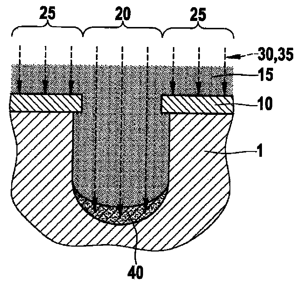
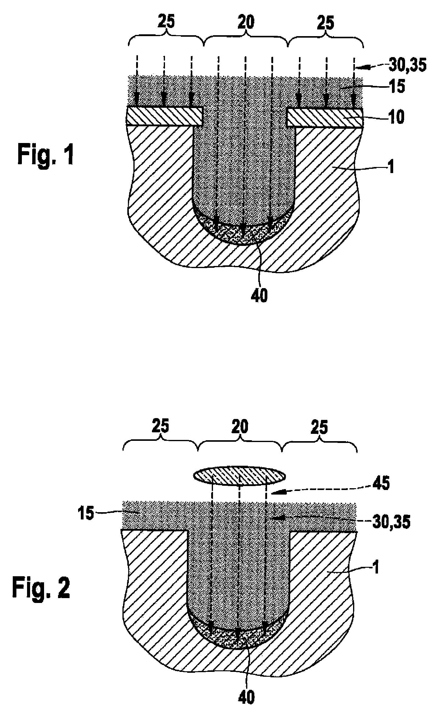
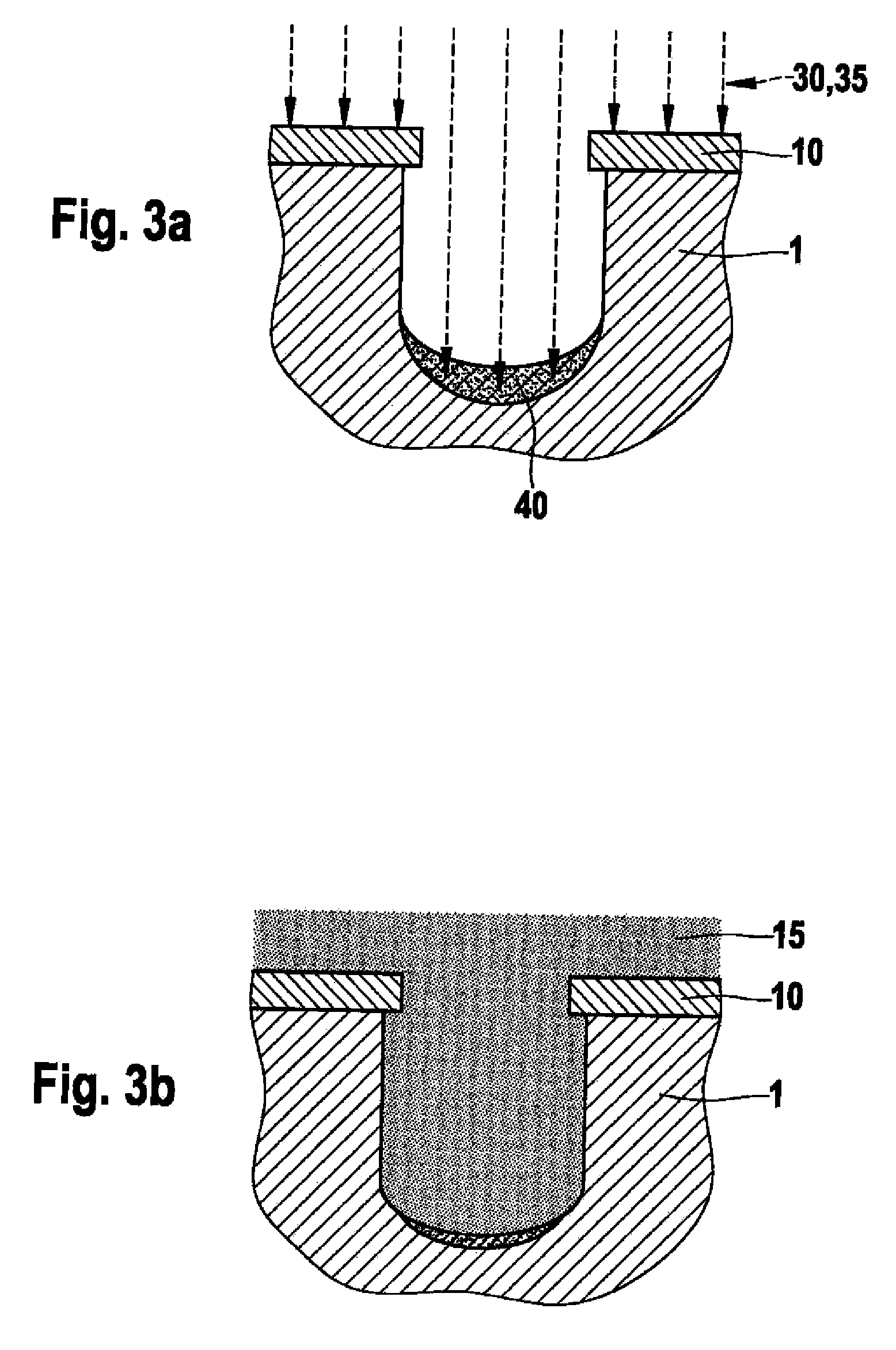
[0012]The method according to example embodiments of the present invention is based on the feature that the mixed semiconductor SiGe may be etched significantly more rapidly than Si. In addition, the superior higher etching rate for SiGe already occurs with a small proportion of germanium, for example, already from 3% germanium.

[0013]Therefore, for plasma-free etching of silicon having one or more areas to be etched, it is provided that the silicon be converted into the mixed semiconductor SiGe by introducing germanium and etched by supplying the etching gas ClF3 or XeF2. The method very advantageously allows the introduction of germanium and the supply of the etching gas ClF3 or XeF2 to be performed at the same time or, if needed, also alternatingly. In both cases, it is possible to introduce germanium selectively only at the areas of the silicon to be etched.

[0014]The variations of the general method will now be explained on the basis of examples. Although the silicon is provided ...


PUM

PropertyMeasurementUnit
Timeaaaaaaaaaa
Structureaaaaaaaaaa
Areaaaaaaaaaaa

Abstract

A method for the plasma-free etching of silicon using the etching gas ClF3 or XeF2 and its use are provided. The silicon is provided having one or more areas to be etched as a layer on the substrate or as the substrate material itself. The silicon is converted into the mixed semiconductor SiGe by introducing germanium and is etched by supplying the etching gas ClF3 or XeF2. The introduction of germanium and the supply of the etching gas ClF3 or XeF2 may be performed at the same time or alternatingly. In particular, it is provided that the introduction of germanium be performed by implanting germanium ions in silicon.

Description

FIELD OF THE INVENTION[0001]The present invention relates to a method for plasma-free etching of silicon using the etching gas ClF3 or XeF2 and its use.BACKGROUND INFORMATION[0002]In semiconductor technology, etching procedures are among the most essential processing technologies for the targeted removal of materials. The etching of silicon is a known and important processing step both in electronic circuit technology and also in microsystem technology. However, it is fundamentally different in principle that the manufacture of an electronic circuit typically represents a planar problem, while micromechanical components typically are three-dimensional, i.e., the structuring depth is unequally pronounced. The etching of defined, in particular spatially narrow areas in depth is therefore among the fundamental technologies, in particular in microsystem technology. A demand for an etching method having greater etching speed results therefrom.[0003]A deep etching method for silicon is de...

Claims


Application Information

Patent Timeline
IPC IPC(8): H01L21/306
CPCB81C1/00531B81C2201/0135H01L21/26506H01L21/266H01L21/3065H01L21/32135H01L21/78
Inventor BENZEL, HUBERTPINTER, STEFANSCHELLING, CHRISTOPHPIRK, TJALFGONSKA, JULIANKLOPF, FRANKLEINENBACH, CHRISTINA
Owner ROBERT BOSCH GMBH
Features
  • Generate Ideas
  • Intellectual Property
  • Life Sciences
  • Materials
  • Tech Scout
  • Unparalleled Data Quality
  • Higher Quality Content
  • 60% Fewer Hallucinations
Learn More