Multipath accessible semiconductor memory device

a memory device and multi-path technology, applied in the direction of memory adressing/allocation/relocation, instruments, digital computers, etc., can solve the problems of increasing the size and cost of a corresponding memory configuration, and affecting the speed of data transmission

Inactive Publication Date: 2008-10-16
SAMSUNG ELECTRONICS CO LTD
View PDF6 Cites 63 Cited by
  • Summary
  • Abstract
  • Description
  • Claims
  • Application Information

AI Technical Summary

Benefits of technology

[0010]Exemplary embodiments of the present invention are directed to a semiconductor memory device having an interfacing function between multiple processors capable of indirectly controlling a flash memory. In an exemplary embodiment, the semiconductor memory device includes a shared memory area accessed by first and second processors via different input/output ports. The shared memory area is allocated to a portion of a memory cell array. A flash memory is located outside the shared memory area and is coupled to the second proc...

Problems solved by technology

Although UART, SPI, and SRAM interfaces may also be used, they can only accommodate low speed transmission.
Thus, it is difficult to ensure a satisfactory data transmission speed which increases the size and cost of a corresponding memory configuration.
Such interf...

Method used


Image

  • Multipath accessible semiconductor memory device
  • Multipath accessible semiconductor memory device
  • Multipath accessible semiconductor memory device

Examples


Embodiment Construction

[0024]The present invention will now be described more fully hereinafter with reference to the accompanying drawings, in which preferred embodiments of the invention are shown. This invention, however, may be embodied in many different forms and should not be construed as limited to the embodiments set forth herein. Rather, these embodiments are provided so that this disclosure will be thorough and complete, and will fully convey the scope of the invention to those skilled in the art. In the drawings, like numbers refer to like elements throughout.

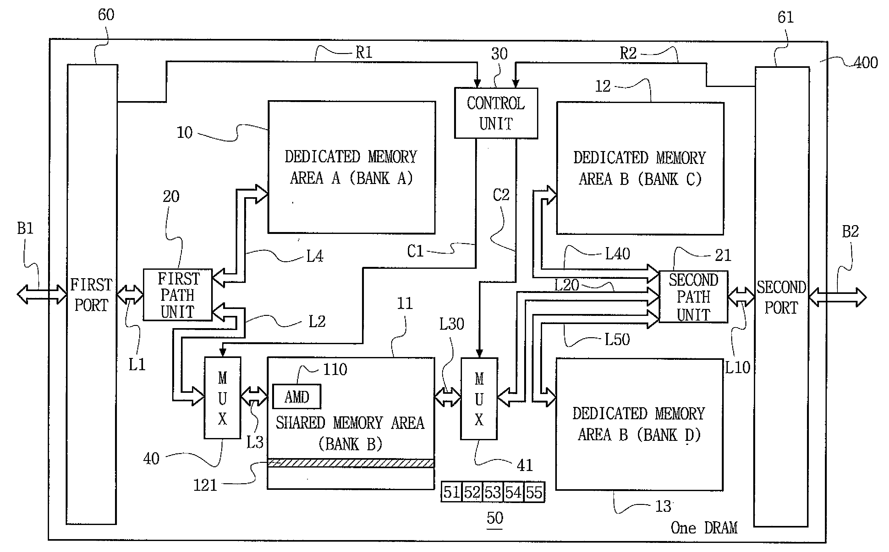
[0025]FIG. 3 is a block diagram of multiprocessor system having a multipath accessible DRAM with a shared use of flash memory according to an embodiment of the invention. A multipath accessible DRAM 400 is coupled between first processor 100 and second processor 200. First processor 100 may be used for application processes and second processor 200 may be an ASIC (Application Specific Integrated Circuit). DRAM 400 may also be, for example,...


PUM


Abstract

A multipath accessible semiconductor memory device provides an interfacing function between multiple processors which indirectly controls a flash memory. The multipath accessible semiconductor memory device comprises a shared memory area, an internal register and a control unit. The shared memory area is accessed by first and second processors through different ports and is allocated to a portion of a memory cell array. The internal register is located outside the memory cell array and is accessed by the first and second processors. The control unit provides storage of address map data associated with the flash memory outside the shared memory area so that the first processor indirectly accesses the flash memory by using the shared memory area and the internal register even when only the second processor is coupled to the flash memory. The control unit also controls a connection path between the shared memory area and one of the first and second processors. The processors share the flash memory and a multiprocessor system is provided that has a compact size, thereby substantially reducing the cost of memory utilized within the multiprocessor system.

Description

CROSS-REFERENCE TO RELATED APPLICATION[0001]This application claims the benefit of Korean Patent Application No. 10-2007-0035485 filed on Apr. 11, 2007, the disclosure of which is incorporated in its entirety by reference.BACKGROUND OF THE INVENTION[0002]1. Field of the Invention[0003]Embodiments of the invention relate to semiconductor memory devices. More particularly, embodiments of the invention relate to a multipath accessible semiconductor memory device adaptable between a plurality of processors.[0004]2. Discussion of Related Art[0005]In general, a semiconductor memory device having a plurality of access ports is called a multiport memory. A memory device having two access ports is called a dual-port memory. A typical dual-port memory is used as an image processing video memory having a RAM (Random Access Memory) port accessible in a random sequence and a SAM (Serial Access Memory) port accessible only in a serial sequence. A dynamic random access memory (DRAM) is configured ...

Claims


Application Information

Patent Timeline
IPC IPC(8): G06F12/02
CPCG06F15/167G06F2212/2022G11C16/04G11C16/08G11C16/06
Inventor KWON, JIN-HYOUNGSOHN, HAN-GULEE, DONG-WOO
Owner SAMSUNG ELECTRONICS CO LTD
Why Eureka
Try Eureka