Structure for Preventing Peeling of Reaction Product, Process for Its Production and Process for the Production of a Semiconductor Device Using the Structure

Inactive Publication Date: 2008-10-23
TEXAS INSTR INC
View PDF2 Cites 16 Cited by
  • Summary
  • Abstract
  • Description
  • Claims
  • Application Information

AI Technical Summary

Benefits of technology

[0007]To accomplish the above objective, the structure for preventing peeling of reaction product of this invention for a plasma treatment device is characterized in that a material to be treated is placed in a chamber, a required treatment gas is introduced into said chamber under vacuum, and the plasma etching of said material to be treated is c

Problems solved by technology

Deposition films of the reaction product on the adhesion preventing plates tend to grow each time the plasma etching process is carried out, the thickness increases, and if they are left alone as they are, the film tends to peel off from the adhesion preventing plates.
The peeled layer forms particles, which may fall on the substrate being treated, causing the product yield to drop.
However, with the use of the adhesion preventing plates of

Method used


Image

  • Structure for Preventing Peeling of Reaction Product, Process for Its Production and Process for the Production of a Semiconductor Device Using the Structure
  • Structure for Preventing Peeling of Reaction Product, Process for Its Production and Process for the Production of a Semiconductor Device Using the Structure
  • Structure for Preventing Peeling of Reaction Product, Process for Its Production and Process for the Production of a Semiconductor Device Using the Structure

Examples


Embodiment Construction

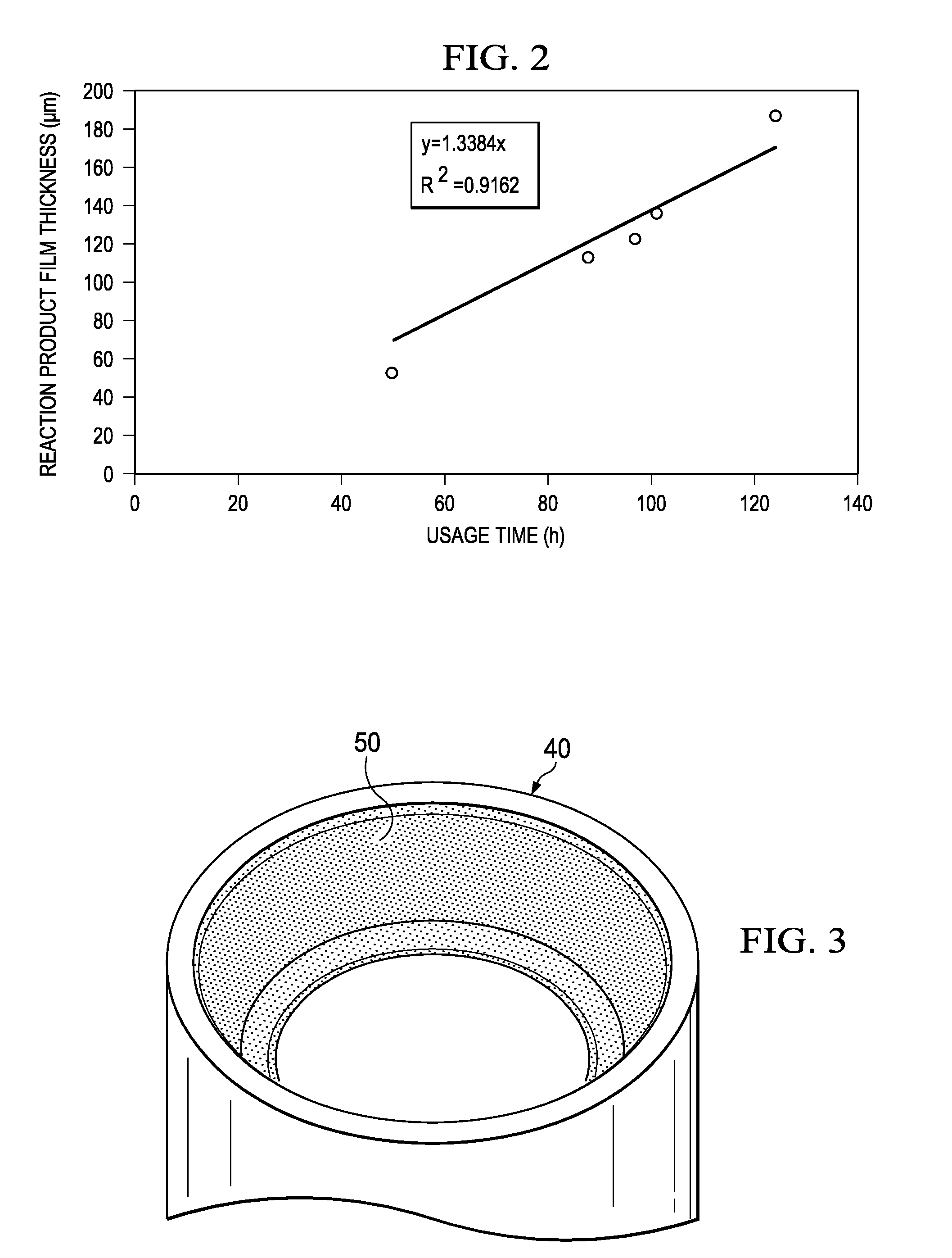
[0022]According to the structure for preventing peeling of reaction product, process for its production and process for the production of a semiconductor device using the structure of this invention, the undesired peeling of reaction product inside the chamber of a plasma etching device is conveniently preventable because of the configuration and action as described above.

[0023]The preferred embodiment of this invention is explained with reference to the attached drawings as follows.

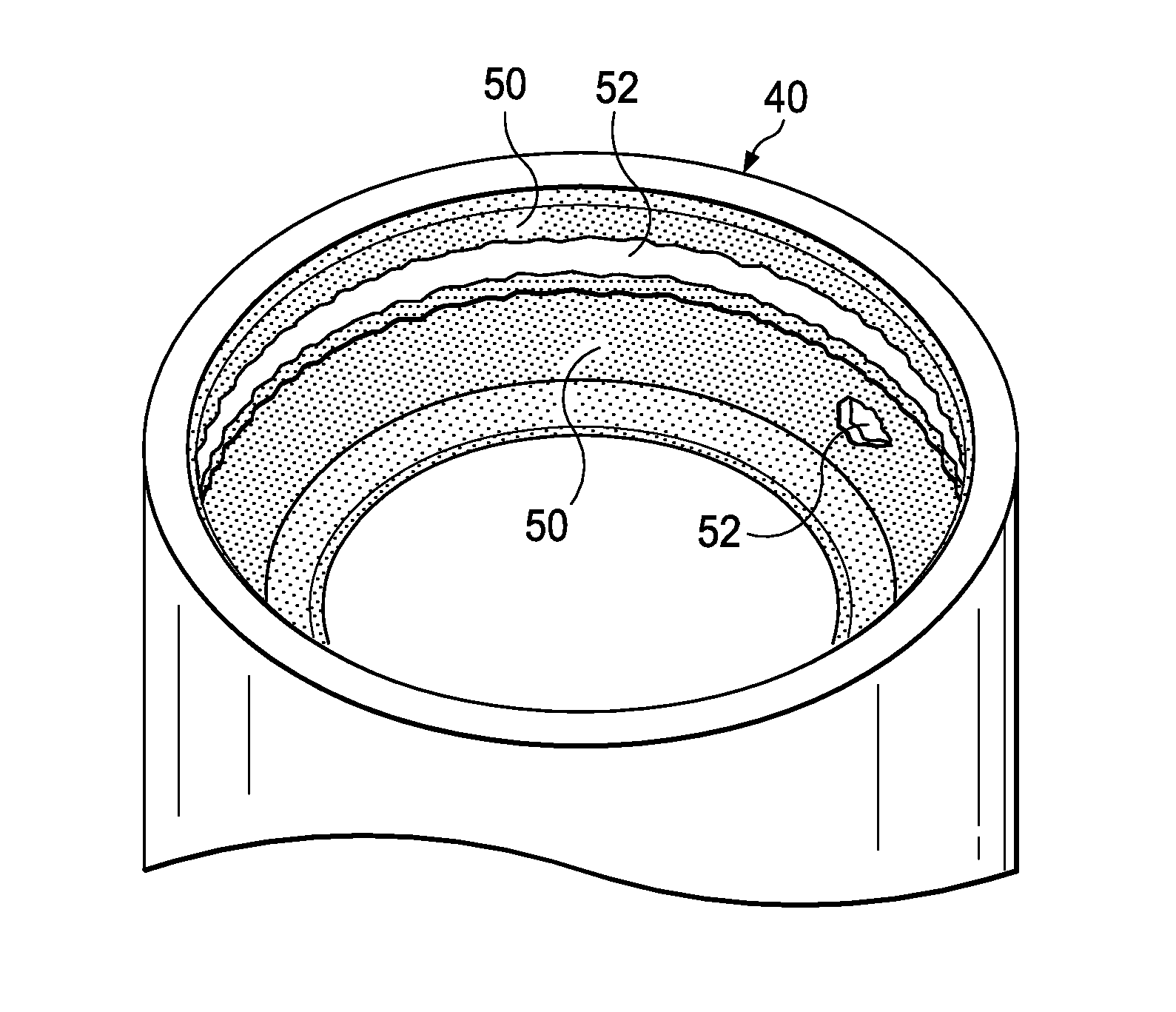
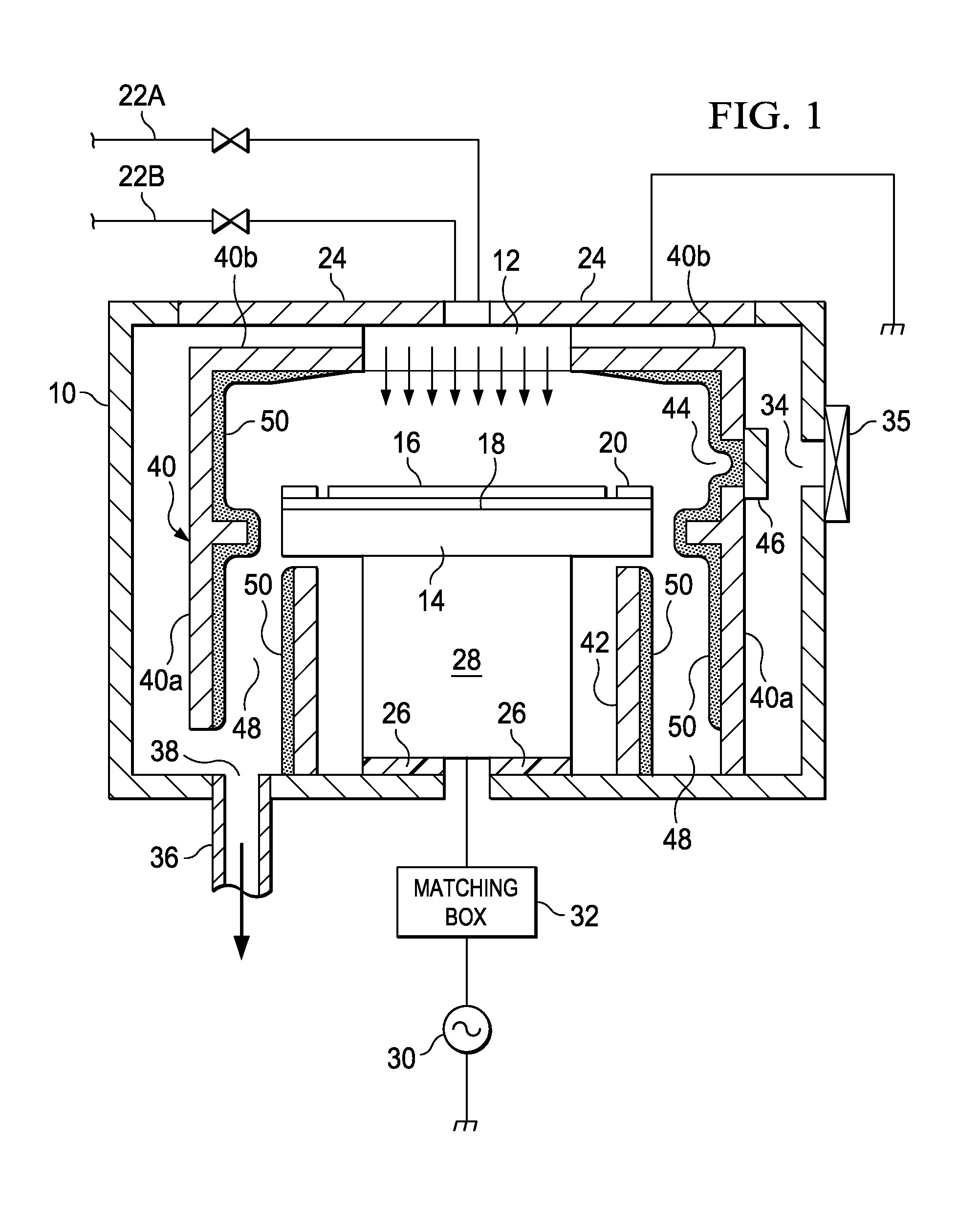
[0024]FIG. 1 shows a configuration of a capacitively coupled plasma etching device with one preferred embodiment of this invention applied. This plasma etching device has a chamber 10 that is a cylindrical hollow body made of aluminum (Al). An interior shower head 12 functioning also as an upper electrode and a susceptor 14 also functioning as a lower electrode are provided on the top and bottom, respectively, in parallel with the required spacing. A material to be treated, for example semiconductor wafe...


PUM

PropertyMeasurementUnit
Lengthaaaaaaaaaa
Mean roughnessaaaaaaaaaa

Abstract

The peeling of a reaction product deposition film 50 is prevented, reducing the particle contamination of a material to be treated 16 by roughening the surfaces (adhesion preventing surfaces) of an outer liner 40 and inner liner 42 both made of aluminum installed as an adhesion preventing plate inside a chamber of a plasma etching device to a surface roughness within a constant range without carrying out alumite treatment.

Description

FIELD OF THE INVENTION[0001]This invention pertains to the prevention of particle contamination on a material to be treated inside the chamber of a treatment device. In particular, it pertains to a reaction product peeling structure that can be used to prevent the formation of particles attributable to the reaction product inside a plasma etching device, a process for its production and a process for the production of a semiconductor device using the structure.BACKGROUND OF THE INVENTION[0002]The etching technique used in the production of semiconductor devices, liquid crystal displays, etc., involves masking a resist pattern formed on the surface of a material to be treated by lithography and processing a thin film of the resist to the desired circuit pattern. It is an essential process. In the main stream plasma etching process being carried out currently, a reactive treatment gas is ionized and dissociated with high-frequency discharge inside a chamber (treatment container) under...

Claims


Application Information

Patent Timeline
IPC IPC(8): D06N7/04C23F4/00B24C1/00
CPCB24C1/06H01J37/32477H01J37/32623Y10T428/24355H01L21/67069H01L21/67253Y10T428/12993H01J2237/334
Inventor SHISHIKURA, HIROTSUGU
Owner TEXAS INSTR INC
Why Eureka
Try Eureka