Process for Fabricating Optical Waveguides

a technology of optical waveguides and fabrication processes, applied in the field of optical waveguides, can solve the problems of failure to meet expectations on the basis of cost, low yield and expensive products, and produces devices with moderate insertion loss, and achieve the effect of improving the process for fabricating optical waveguides

Inactive Publication Date: 2008-10-30
CORP DE LECOLE POLYTECHNIQUE DE MONTREAL
View PDF10 Cites 30 Cited by
  • Summary
  • Abstract
  • Description
  • Claims
  • Application Information

AI Technical Summary

Benefits of technology

[0007]An object of the present invention is therefore to pro

Problems solved by technology

Many of these failed to meet expectations on grounds of cost.
Until recently, devices were based on fibre or free-space, both of which require careful alignment and subcomponent selection; resulting in low yields and expensive products caused mainly by the remaining intensive labour.
Even though there is currently considerable interest in the potential of this technology, it produces devices with moderate insertion loss due to the fabrication technique as well as in/out coupling.
Another drawback of current planar optic manufacturing process is that it involves expensive facilities to perform the micro-fabrication and places considerable limitations on the types of materials that can be used for the substrates.
However, this technique is limited t

Method used


Image

  • Process for Fabricating Optical Waveguides
  • Process for Fabricating Optical Waveguides
  • Process for Fabricating Optical Waveguides

Examples


Embodiment Construction

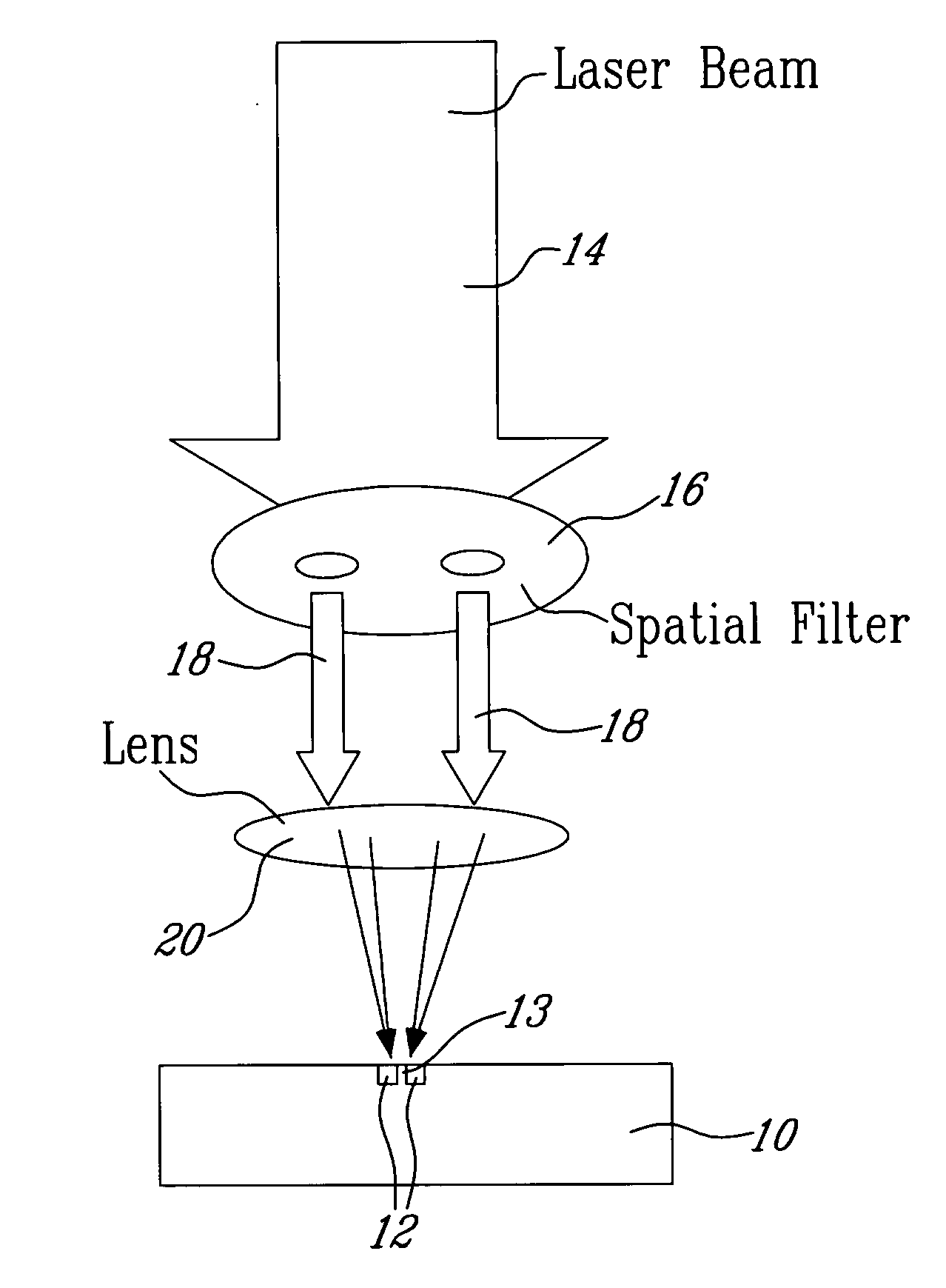
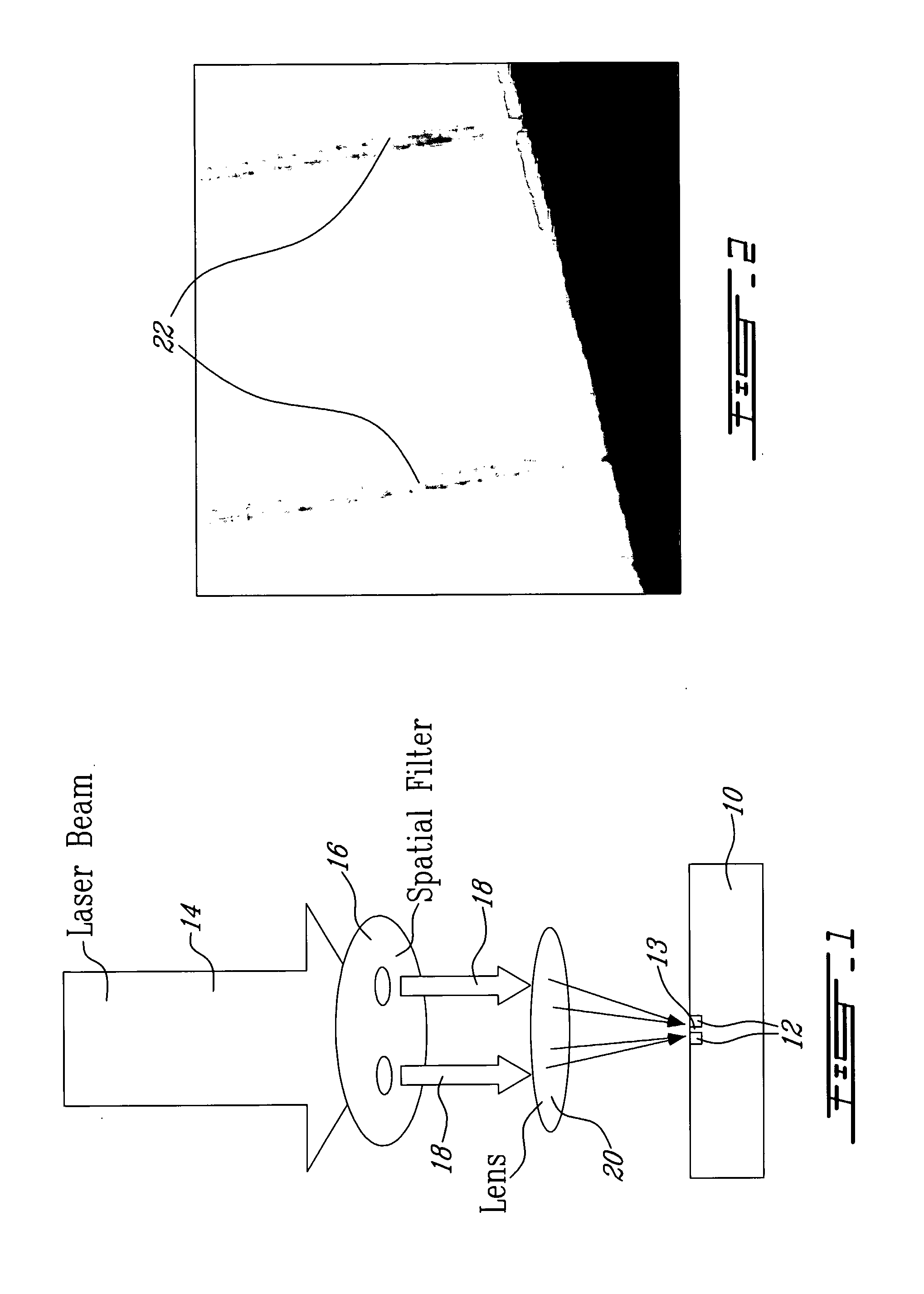
[0042]A process and system for fabricating planar waveguides according to a first illustrated embodiment of the present invention will now be described with reference to FIG. 1.

[0043]A high power laser, for example of the CO2 type (not shown), is used to cut into a substrate material in our current embodiment in the form of a glass plate 10, two substantially parallel channels 12, defining a ridge waveguide 13 there between.

[0044]It is to be noted that the substrate material may be a metal, a semiconductor or a dielectric.

[0045]More specifically, the CO2 laser produces a beam 14 of a 10.6 micron wavelength which is split through a spatial filter 16 producing two parallel beams 18 that are focused through a lens 20 onto the surface of the substrate 10. It is believed to be within the reach of a person skilled in the art to adequately select the spatial filter 16 and lens 20 so as to yield a desired distance between the two channels 12. Of course the dimensions of the two channels 12 ...


PUM

PropertyMeasurementUnit
Temperatureaaaaaaaaaa
Dielectric polarization enthalpyaaaaaaaaaa
Poweraaaaaaaaaa

Abstract

A one step process for fabricating planar optical waveguides comprises using a laser to cut at least two channels in a substantially planar surface of a piece of dielectric material defining a waveguide there between. The shape and size of the resulting guide can be adjusting by selecting an appropriate combination of laser beam spatial profile, of its power and of the exposure time. A combination of heating and writing lasers can also be used to fabricate waveguides in a dielectric substrate, wherein the heating laser heats the substrate with a relatively broad focused spot, the power of the heating laser being controlled to raise the temperature heating the substrate just below the substrate's threshold temperature at which it begins to absorb electro-magnetic radiation, the writing laser, which yields a spot size smaller than the heating laser then melts the substrate within the focal spot of the heating laser. Compare to processes from the prior art, a waveguide fabrication process according to the present invention results in lower cost, faster processing time and applicability to a wider range of materials. The present process is particularly suited for the mass production of inexpensive photonic devices.

Description

FIELD OF THE INVENTION[0001]The present invention relates to optical waveguides. More specifically, the present invention is concerned with a process for fabricating planar optical waveguides.BACKGROUND OF THE INVENTION[0002]For many years, the photonics industry has grown steadily primarily driven by the increasing demand for complex optical functionality. More recently, the need to save space and lower cost of deployment has overtaken the requirement for developing optical devices. Many new promising optical devices were proposed to create an all-optical network with novel passive and active optical devices to modify the transmitted information. Many of these failed to meet expectations on grounds of cost.[0003]Until recently, devices were based on fibre or free-space, both of which require careful alignment and subcomponent selection; resulting in low yields and expensive products caused mainly by the remaining intensive labour. More recently, planar optical integrated circuits w...

Claims


Application Information

Patent Timeline
IPC IPC(8): B23K26/36B23K26/364
CPCB23K26/0613B23K26/067B23K26/4065B23K26/4075C03C23/0025G02B6/10G02B6/13B23K26/40B23K2103/42B23K2103/50
Inventor KASHYAP, RAMANTREANTON, VINCENT
Owner CORP DE LECOLE POLYTECHNIQUE DE MONTREAL
Why Eureka
Try Eureka