Embedded silicon germanium using a double buried oxide silicon-on-insulator wafer

a technology of silicon germanium and oxide silicon, applied in the field of ptype field effect transistor, can solve the problems of large yield issue, thick silicon germanium layer, and even more difficult enhancement of hole mobility, so as to increase longitudinal stress, increase longitudinal stress, and increase longitudinal stress in the channel region

Inactive Publication Date: 2008-10-30
GLOBALFOUNDRIES US INC
View PDF32 Cites 16 Cited by
  • Summary
  • Abstract
  • Description
  • Claims
  • Application Information

AI Technical Summary

Benefits of technology

[0009]A method of forming a p-type field effect transistor of the present invention comprises providing a double BOX SOI wafer. An n-doped portion is formed in the first silicon layer and a gate stack for the p-type field effect transistor is formed on the n-doped portion. Temporary sidewall spacers are formed on the gate stack. Trenches are then lithographically patterned into the wafer on either side of the sidewall spacers on the gate stack. The trenches are then etched through to the second silicon layer by first selectively etching a recess in the first silicon layer to expose the first buried oxide layer. Then, another recess is selectively etched through the first buried oxide layer to expose the second silicon layer. Strained silicon germanium is formed in the trenches in order to impose a longitudinal stress on a channel region in the first silicon layer between the trenches. The strained silicon germanium can be formed in the trenches by epitaxially growing the strained silicon germanium from the second silicon layer exposed when the trenches were formed. The strained silicon germanium may be grown above a top surface of wafer in order to further increase the longitudinal stress on the channel region. The strained silicon germanium may also be in situ doped with boron during the epitaxial growth process so that the source / drain regions comprise the necessary p-doped silicon for a p-type field effect transistor. The temporary sidewall spacers are removed and additional processing continues until the p-type field effect transistor is completed (e.g., source / drain extension implantation, permanent sidewall spacers formation on the gate stack, silicide formation on the source / drain regions and the gate stack, implantation anneal, etc.)

Problems solved by technology

However, this technique requires silicon germanium to be relaxed, which demands a very thick silicon germanium layer (i.e., 0.5-1 micron) in bulk systems.
These dislocations are known to cause a major yield issue.
Hole mobility is even more difficult to enhance in this approach since we need a very large germanium percentage in the relaxed silicon germanium film which causes an even bigger yield and dislocation problem.
Unfortunately, in the SGOI system, as the silicon germanium relaxes, dislocations (and in addition, stacking faults) form with concomitant yield degradation.
Further, the cost of the process is also prohibitive.
Some techniques such as graded germanium concentration and chemical mechanical polishing (CMP) are used to improve the quality of the films, but in general, this process is plagued by a high density of defects and prohibitive costs.

Method used


Image

  • Embedded silicon germanium using a double buried oxide silicon-on-insulator wafer
  • Embedded silicon germanium using a double buried oxide silicon-on-insulator wafer
  • Embedded silicon germanium using a double buried oxide silicon-on-insulator wafer

Examples


Embodiment Construction

[0023]The present invention and the various features and advantageous details thereof are explained more fully with reference to the nonlimiting embodiments that are illustrated in the accompanying drawings and detailed in the following description. It should be noted that the features illustrated in the drawings are not necessarily drawn to scale. Descriptions of well-known components and processing techniques are omitted so as to not unnecessarily obscure the present invention. The examples used herein are intended merely to facilitate an understanding of ways in which the invention may be practiced and to further enable those of skill in the art to practice the invention. Accordingly, the examples should not be construed as limiting the scope of the invention.

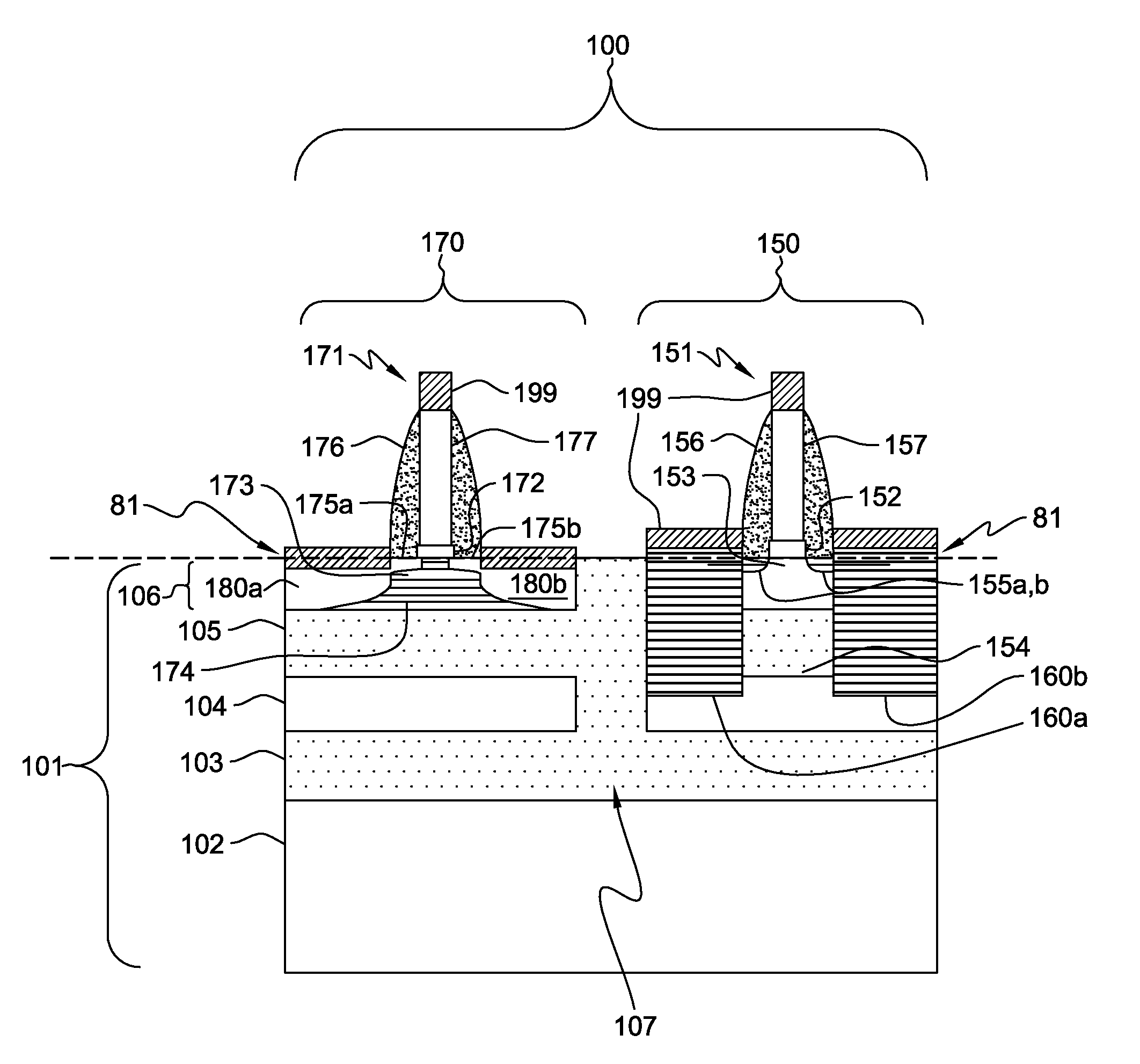
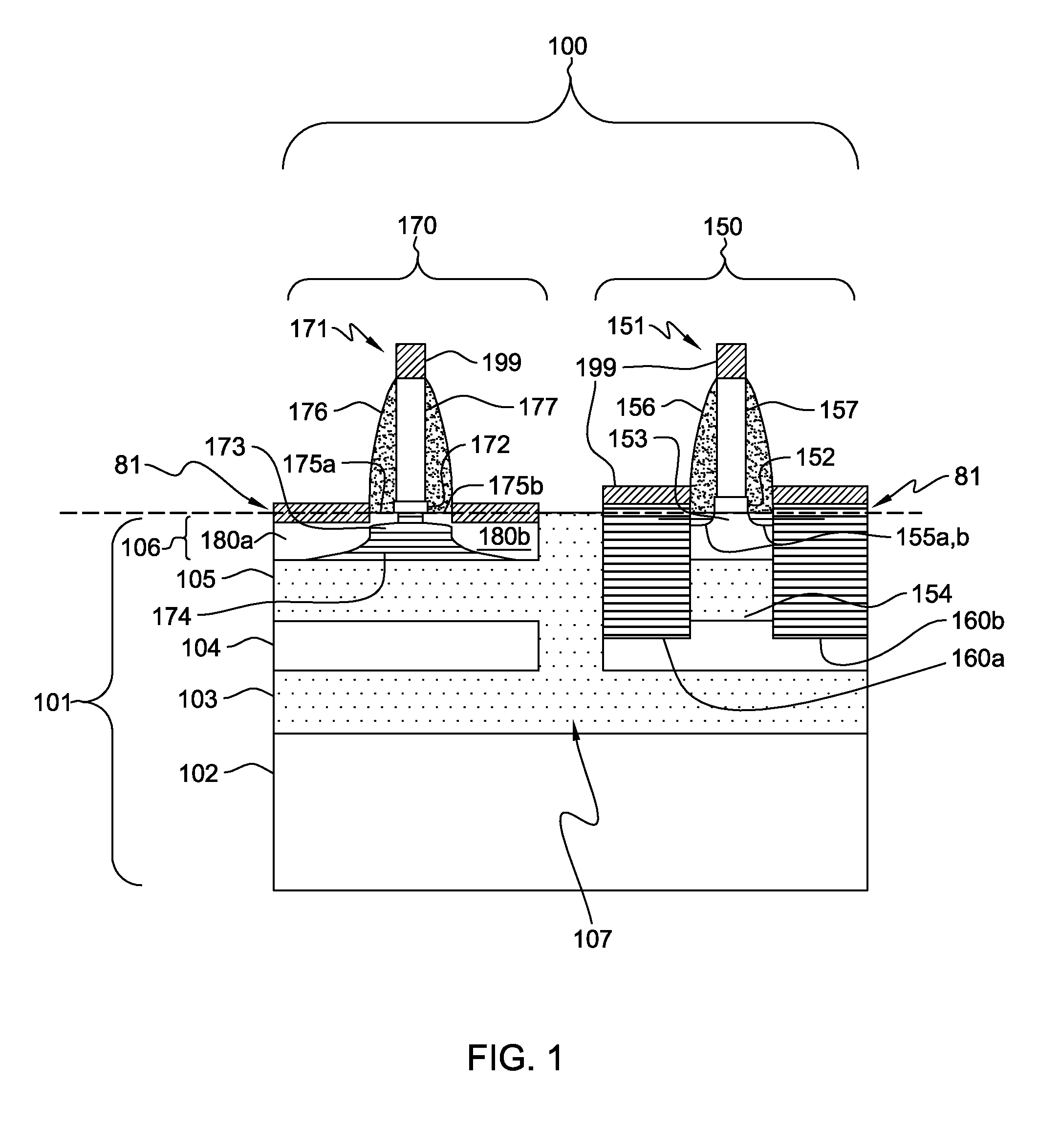
[0024]As discussed above, strain in the silicon channel can affect the mobility of CMOS transistor carriers significantly. Compressive longitudinal stress along the channel is known to help the pFET (P-type field effect tran...


PUM


Abstract

Disclosed is a p-type field effect transistor (pFET) structure and method of forming the pFET. The pFET comprises embedded silicon germanium in the source / drain regions to increase longitudinal stress on the p-channel and, thereby, enhance transistor performance. Increased stress is achieved by increasing the depth of the source / drain regions and, thereby, the volume of the embedded silicon germanium. The greater depth (e.g., up to 100 nm) of the stressed silicon germanium source / drain regions is achieved by using a double BOX SOI wafer. Trenches are etched through a first silicon layer and first buried oxide layer and then the stressed silicon germanium is epitaxially grown from a second silicon layer. A second buried oxide layer isolates the pFET.

Description

CROSS-REFERENCE TO RELATED APPLICATIONS[0001]This application is a continuation of U.S. application Ser. No. 10 / 908,394 filed May 10, 2005.BACKGROUND OF THE INVENTION[0002]1. Field of the Invention[0003]The invention generally relates to a p-type field effect transistor and a method of forming the transistor using a double buried oxide silicon-on-insulator wafer that allows for a thick growth of strained silicon germanium in the source / drain regions to create longitudinal stress on the channel region.[0004]2. Description of the Related Art[0005]U.S. Pat. No. 6,621,131 to Murthy (hereinafter “Murthy”) discloses embodiments that were satisfactory for the purposes for which they were intended. The disclosure of Murthy, in its entirety, is hereby expressly incorporated by reference into the present invention for purposes including, but not limited to, indicating the background of the present invention and illustrating the state of the art. It has been shown that the strain in the silico...

Claims


Application Information

Patent Timeline
Patent Type & Authority Applications(United States)
IPC IPC(8): H01L27/12
CPCH01L27/1203H01L29/66628H01L29/66636H01L29/7842H01L29/7848H01L29/78603H01L29/78618H01L29/78684
Inventor CHEN, HUAJIECHIDAMBARRAO, DURESETISCHEPIS, DOMINIC J.UTOMO, HENRY K.
Owner GLOBALFOUNDRIES US INC
Why Eureka
Try Eureka