Solid-State Imaging Device, Optical Sensor and Method of Operating Solid-State Imaging Device

a solid-state imaging and optical sensor technology, applied in the field of solid-state imaging devices, optical sensors and methods of operating solid-state imaging devices, can solve the problems of low sensitivity, degraded s/n ratio, difficulty in matching both images, etc., and achieve low illuminance, high s/n ratio, and high sensitivity

Active Publication Date: 2008-10-30
TOHOKU UNIV
View PDF8 Cites 78 Cited by
  • Summary
  • Abstract
  • Description
  • Claims
  • Application Information

AI Technical Summary

Benefits of technology

[0113]With the solid-state imaging device according to the present invention, the photodiode generates the photoelectric charges upon receipt of light and accumulates the same and keeps high sensitivity in low illuminance with a high S/N ratio. Additionally, the storage capacitor element accumulates the photoelectric charges overflowing from the photodiode for thereby enabling the shooting

Problems solved by technology

However, according to the methods disclosed in the Patent Documents 1, 2, 3 and the Non-Patent Document 2, mentioned above, or the method of performing the double shooting for different exposure times, the shootings for low illuminance and high illuminance need to be performed at different times. Therefore, a difference exists in moving images resulting from the shootings performed in respective illuminance and an issue occurs with a difficulty caused in matching both of the images.
Further, with the methods disclosed in Patent-Document 4 and Non-Patent Document 3 mentioned above, even though a sche

Method used


Image

  • Solid-State Imaging Device, Optical Sensor and Method of Operating Solid-State Imaging Device
  • Solid-State Imaging Device, Optical Sensor and Method of Operating Solid-State Imaging Device
  • Solid-State Imaging Device, Optical Sensor and Method of Operating Solid-State Imaging Device

Examples


first embodiment

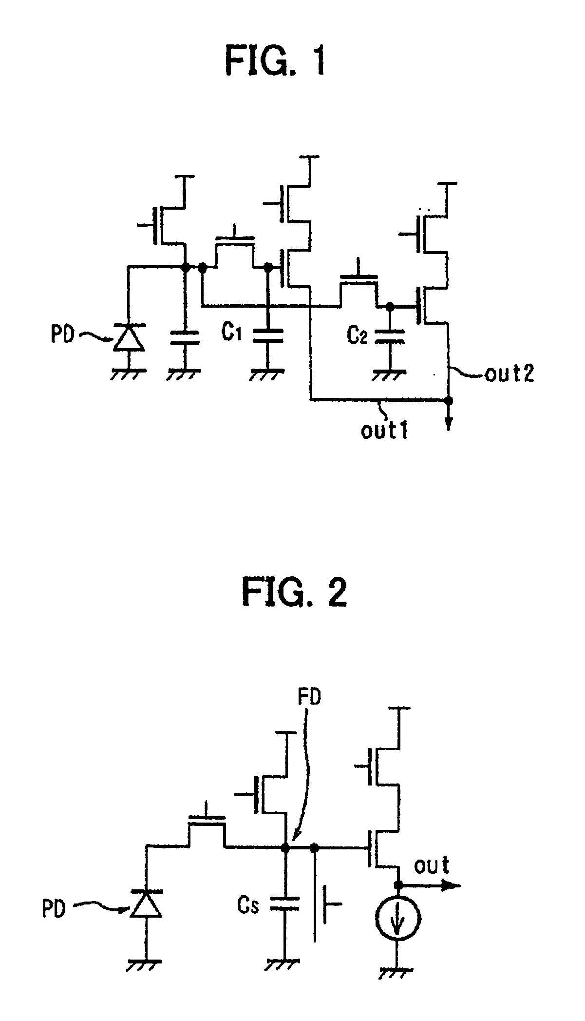
[0154]A solid-state imaging device of the present embodiment is structured in the form of a CMOS image sensor and FIG. 6 is an equivalent circuit diagram for one pixel.

[0155]Each pixel includes a photodiode PD for receiving light and generating photoelectric charges, a transfer transistor Tr1 for transferring the photoelectric charges of the photodiode PD, a floating diffusion region FD from which the photoelectric charges are transferred via the transfer transistor Tr1, a storage capacitor element Cs for accumulating the photoelectric charges overflowing from the photodiode during accumulating operation, a storage transistor Tr2 for coupling or splitting potentials of the floating diffusion region FD and the storage capacitor element Cs, a reset transistor Tr3 coupled to the floating diffusion region FD for discharging the photoelectric charges of the floating diffusion region FD, an amplifier transistor Tr4 for amplifying the photoelectric charges of the floating diffusion region ...

second embodiment

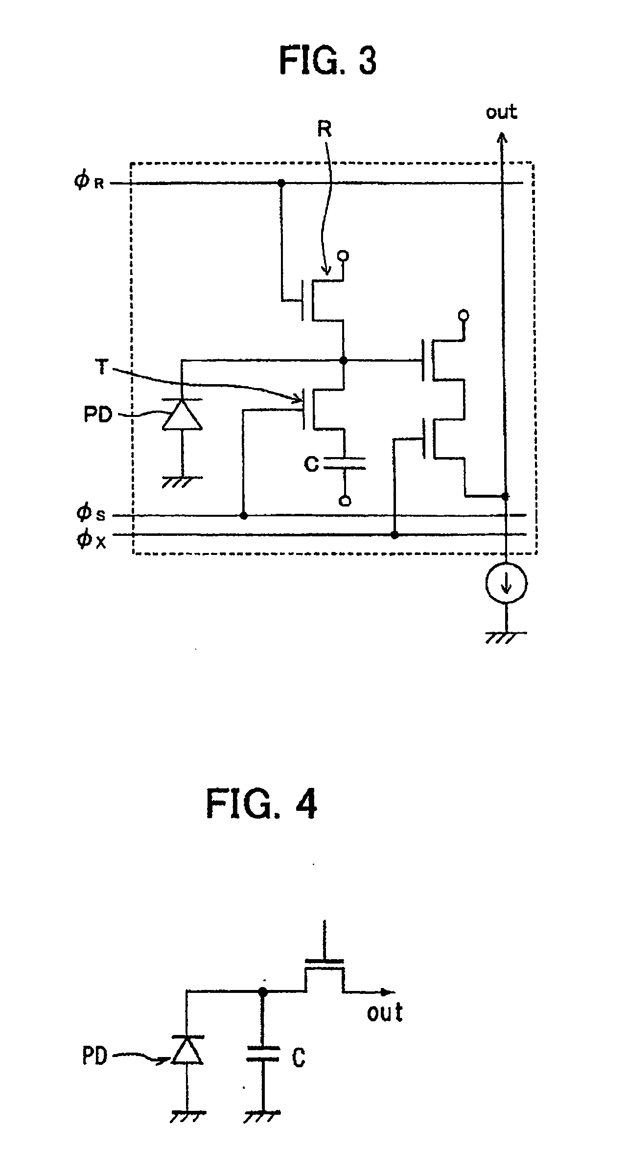
[0234]A CMOS image sensor of the present embodiment is similar to the CMOS image sensor of the first embodiment but differs therefrom in a driving method.

[0235]FIG. 16 is a timing chart showing voltages applied to the drivelines (ΦT, ΦS, ΦR) each with two levels in on / off states. Like the first embodiment, ΦT may take three levels additionally including a level (+α).

[0236]First, at time T0 when a new filed begins, ΦR is set to be on under a status where ΦT is set to be off and ΦS is set to be on. This causes the photoelectric charges created in a preceding field to be discharged for resetting.

[0237]The accumulation time period TPD for CPD begins at a time point when ΦT is set to be off to allow CPD to start accumulating the photoelectric charges.

[0238]Next, at time T1 immediately after the resetting at time T0, ΦR is set to be off. At this moment, CFD and CS are brought into a coupled condition and a signal of CFD+CS at a reset level is read out as noise N2 for storage in the frame ...

third embodiment

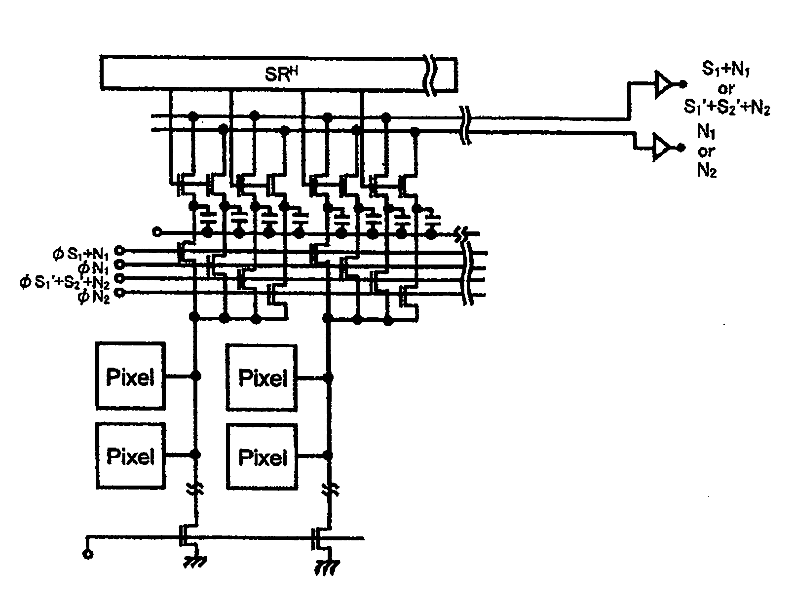
[0271]In the CMOS image sensors of the first and second embodiments or the CMOS image sensor of the first embodiment having a pattern in which the storage-capacitor-element accumulation period TCS begins at time T0, the signal at the reset level of CFD+CS is read out as noise N2 and accumulated in the frame memory FM. This enables the canceling of noise appearing when sampling the signal of the sum (S1+S2) of the pre-saturated charge signal and the supersaturated charge signal. On the contrary, a CMOS image sensor of the present embodiment enables a reduction in cost of a chip without using the frame memory.

[0272]The frame memory is needed because the sampling timing of the signal (N2) at the reset level of CFD+CS precedes the sampling timing of the sum (S1′+S2′+N2) of the modulated pre-saturated charge signal and the supersaturated charge signal by one frame.

[0273]Here, the signal (N1) at the reset level of CFD+CS may be replaced by the signal (N1) at the reset level of CFD or the ...


PUM


Abstract

A solid-state imaging device and an optical sensor, which can enhance a wide dynamic range while keeping a high sensitivity with a high S/N ratio, and a method of operating a solid-state imaging device for enhancing a wide dynamic range while keeping a high sensitivity with a high S/N ratio are disclosed. An array of integrated pixels has a structure wherein each pixel comprises a photodiode PD for receiving light and generating and accumulating photoelectric charges and a storage capacitor element CS coupled to the photodiode PD through a transfer transistor Tr1 for accumulating the photoelectric charges overflowing from the photodiode PD. The storage capacitor element CS is structured to accumulate the photoelectric charges overflowing from the photodiode PD in a storage-capacitor-element accumulation period TCS that is set to be a period at a predetermined ratio with respect to an accumulation period of the photodiode PD.

Description

TECHNICAL FIELD[0001]The present invention relates to solid-state imaging devices, optical sensors and methods of operating the solid-state imaging devices and, more particularly, to a solid-state imaging device and an optical sensor of a CMOS type and a method of operating such solid-state imaging device.BACKGROUND ART[0002]Image sensors for an image-input use such as CMOS (Complementary Metal-Oxide-Semiconductor) image sensors or CCD (Charge Coupled Device) image sensors have achieved improvements in performances with an expanding demand for applications in, for instance, digital cameras and cellular phones each equipped with a camera.[0003]The image sensors, described above, need to be further improved in performances, one of which relates to widening a dynamic range.[0004]The conventional image sensor has a dynamic range limited in the order of, for instance, approximately 3 to 4 digits (60 to 80 dB) and does not cover a value of 5 to 6 digits (100 to 120 dB) of the naked eye or...

Claims


Application Information

Patent Timeline
IPC IPC(8): H04N5/335H01L27/146H04N5/355H04N5/369H04N5/374H04N5/3745
CPCH01L27/14609H04N5/3559H04N5/2355H04N3/15H04N23/741H04N25/583H04N25/621H04N25/59H04N25/57
Inventor SUGAWA, SHIGETOSHIADACHI, SATORUYAHATA, KYOICHITERADA, TATSUYA
Owner TOHOKU UNIV
Why Eureka
Try Eureka