Cis Type Thin-Film Solar Cell and Process for Producing the Same

a technology of cis type and solar cells, applied in sustainable manufacturing/processing, climate sustainability, semiconductor devices, etc., can solve the problems of reducing the life of the light absorption layer itself, and achieve the effect of preventing the light absorption layer, improving yield, and reducing the performance of the solar cell

Inactive Publication Date: 2008-11-06
SHOWA SHELL SEKIYU KK
View PDF2 Cites 56 Cited by
  • Summary
  • Abstract
  • Description
  • Claims
  • Application Information

AI Technical Summary

Benefits of technology

[0037]According to the invention, although the step of forming an alkali-barrier layer is newly conducted, a metallic back electrode layer can be successively deposited in the same sputtering apparatus and the excess thermal diffusion of alkali ingredients into the light absorption layer can be prevented and controlled. As a result, the light absorption layer can be prevented from peeling off at the interface of the metallic back electrode layer without reducing solar cell performances (conversion efficiency and open-circuit voltage). Thus, an improved yield and a cost reduction can be attained.
[0038]The invention is applicable to a ceramic target which is an oxide or nitride having no electrical conductivity. According to the invention, two or more deposition steps for depositing different materials can be conducted in the same in-line type sputtering apparatus by depositing a silica layer using a silica target attaining high insulating properties by the RF sputtering method, which has a low deposition rate because a high power cannot be applied, and depositing the first layer of a multilayered metallic back electrode layer successively to the silica layer deposition by the DC sputtering method, in which the deposition rate can be improved by increasing the power to be applied, at the same deposition pressure and the same substrate conveyer speed.
[0039]Furthermore, the invention can eliminate the problems associated with differences in deposition conditions between two different sputtering methods to thereby enable film deposition to be conducted at the same substrate conveyance speed.
[0040]Moreover, according to the invention, film deposition in common argon gas at the same pressure (same argon gas flow rate) is possible. Thus, a two-layer structure can be formed by depositing a silica layer by the RF sputtering method and successively depositing the first layer of a multilayered metallic back electrode layer by the DC sputtering method. By causing this two-layer structure to function as an alkali-barrier layer, a greatly improved deposition rate and a reduction in apparatus cost are attained.
[0041]In addition, since there is no need of purchasing a soda-lime float glass substrate having an alkali-barrier layer, the invention can contribute to a reduction of the cost of a CIS type thin-film solar cell.

Problems solved by technology

Furthermore, in case where sodium, which has deliquescence, comes to be unevenly contained in the light absorption layer, this is a cause of instability or a reduced life of the light absorption layer itself, etc.
However, there are only an extremely small number of publications / reports on an investigation concerning an alkali-barrier layer, and there is no report which teaches the necessity of an alkali-barrier layer in the formation of a light absorption layer by the multi-source co-evaporation method.

Method used


Image

  • Cis Type Thin-Film Solar Cell and Process for Producing the Same
  • Cis Type Thin-Film Solar Cell and Process for Producing the Same
  • Cis Type Thin-Film Solar Cell and Process for Producing the Same

Examples


Embodiment Construction

[0042]Embodiments of the invention will be explained below.

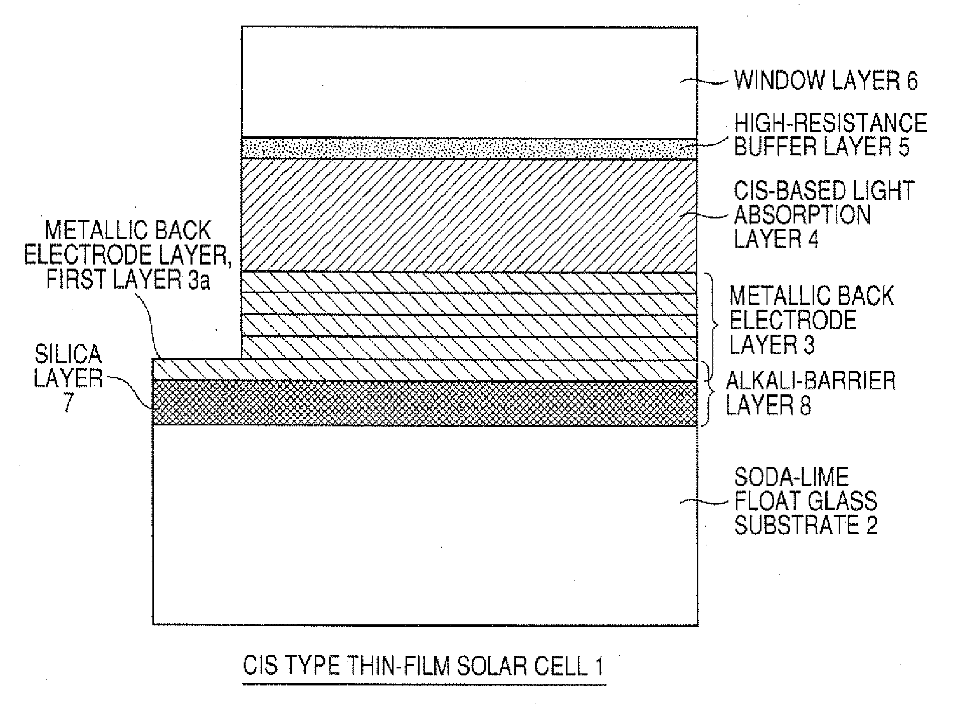
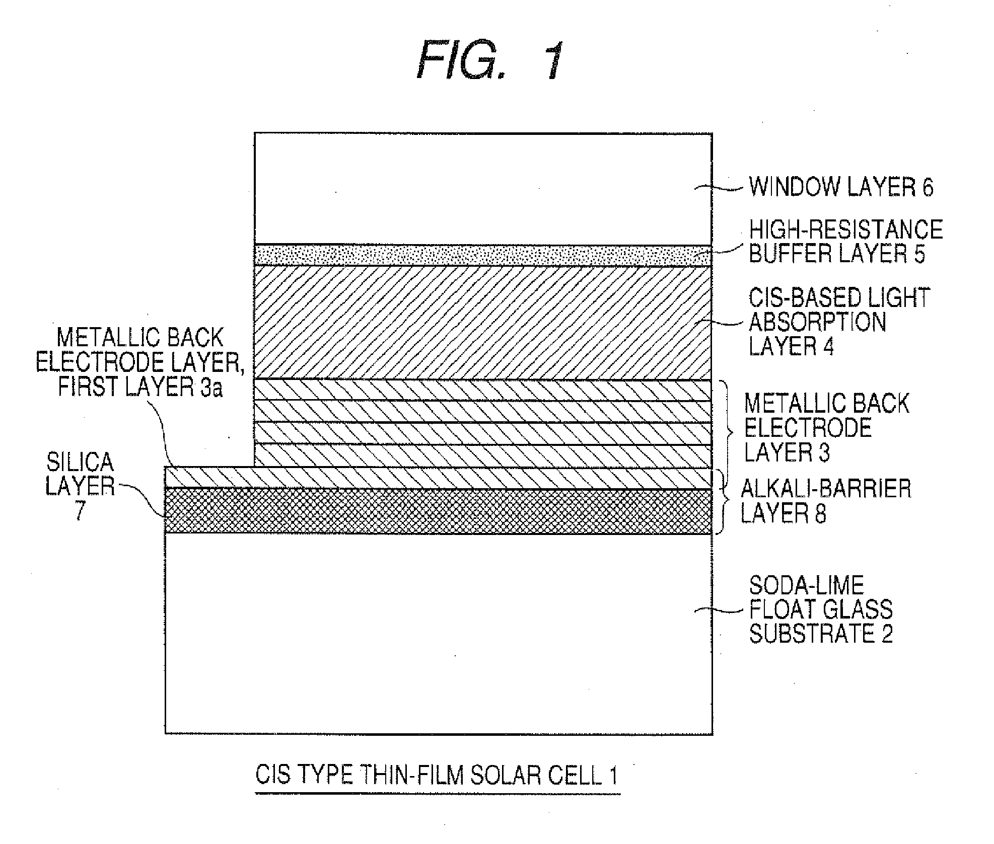
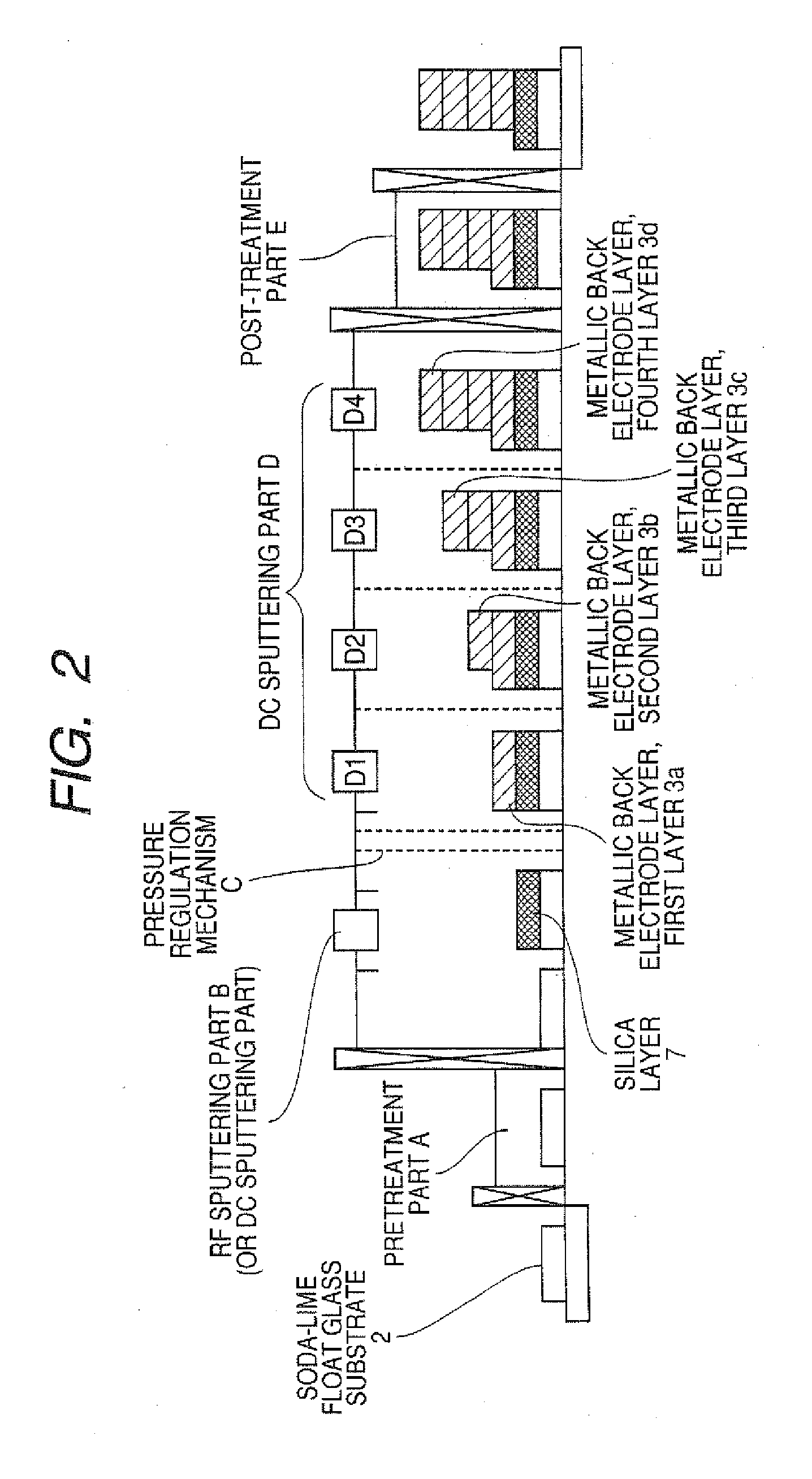
[0043]The invention relates to a method of forming an alkali-barrier layer 8 for preventing and controlling the thermal diffusion of alkali ingredients from a soda-lime float glass substrate 2 into a light absorption layer 4 comprising a p-type semiconductor when the light absorption layer is deposited on a metallic back electrode layer 3 deposited on the soda-lime float glass substrate 2. The invention further relates to a CIS type thin-film solar cell 1 having the alkali-barrier layer 8.

[0044]This alkali-barrier layer 8 may be a first alkali-barrier layer which is a silica layer 7 formed on the soda-lime float glass substrate, or may be a second alkali-barrier layer which is a multilayered alkali-barrier layer composed of the silica layer 7 and the first layer 3a of the multilayered metallic back electrode layer directly overlying the silica layer 7.

[0045]The CIS type thin-film solar cell 1 of the invention has a basic str...


PUM


Abstract

This invention provides a CIS-based thin film solar battery and a process for producing the same in which the formation of an alkali barrier layer and a metal backside electrode layer is carried out at a low cost in a short time to prevent such an unfavorable phenomenon that a light absorbing layer is separated from the interface of the light absorbing layer and the metal backside electrode layer. The CIS-based thin film solar battery (1) comprises a glass substrate (2), an alkali-free layer (7) such as silica, a metal backside electrode layer (3) having a laminate structure, a p-type CIS-based light absorbing layer (4), a high-resistance buffer layer (5), and an n-type window layer (6) stacked in that order. The layer (7), either alone or together with a first layer (3a) in the layer (3), can function as an alkali barrier layer (8) that can prevent and control the thermal diffusion of an alkali component into the light absorbing layer during the formation of the layer (4) from the substrate (2). In the layer (3a), crystal grains are fine and has high density. After the formation of the layer (7) on the substrate by RF or DC sputtering, the layer (3) is continuously formed on the layer (7) by DC sputtering.

Description

TECHNICAL FIELD[0001]The present invention relates to an alkali-barrier layer of a CIS type thin-film solar cell (the alkali-barrier layer, when a light absorption layer is deposited on a metallic back electrode layer, blocks and controls the diffusion of alkali ingredients from the glass substrate underlying the metallic back electrode layer) and to a process for forming the layer.BACKGROUND ART[0002]The invention relates to a CIS type thin-film solar cell having a pn heterojunction comprising: a p-type semiconductor such as a thin multinary-compound semiconductor film, in particular, a I-III-VI2 Group chalcopyrite semiconductor, e.g., copper indium diselenide (CuInSe2), copper indium gallium diselenide (CuInGaSe2), copper gallium diselenide (CuGaSe2), copper indium gallium di-sulfo-sulfide (Cu(InGa)(SSe)2), copper indium disulfide (CuInS2), copper gallium disulfide (CuGaS2), copper indium gallium disulfide (CuInGaS2), or copper indium gallium diselenide (CuInGaSe2) having a thin f...

Claims


Application Information

Patent Timeline
Patent Type & Authority Applications(United States)
IPC IPC(8): H01L31/00
CPCH01L31/0322Y02E10/541H01L31/0749H01L31/03923H01L31/022425Y02P70/50H01L31/0445
Inventor KUSHIYA, KATSUMITANAKA, YOSHIAKIONODERA, MASARUTANAKA, MANABUNAGOYA, YOSHINORI
Owner SHOWA SHELL SEKIYU KK
Why Eureka
Try Eureka