

Variable slot antenna and driving method thereof
a technology of antenna and slot, applied in the direction of slot antenna, antenna, basic electric elements, etc., can solve the problems of large antenna structure, difficult to apply to a communication system, and possible change of antenna
- Summary
- Abstract
- Description
- Claims
- Application Information
AI Technical Summary
Benefits of technology
Problems solved by technology
Method used
Image

Examples
embodiments
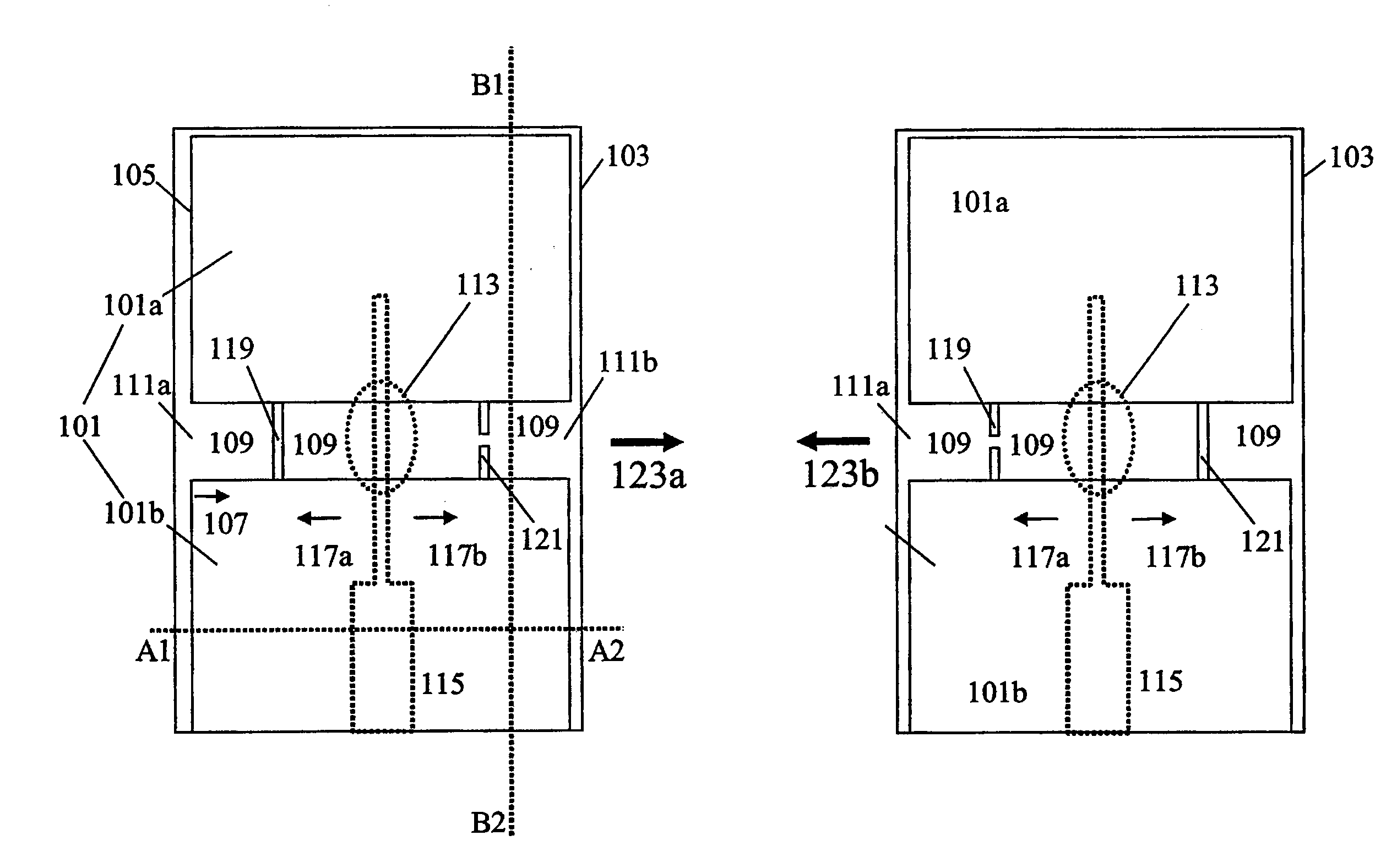
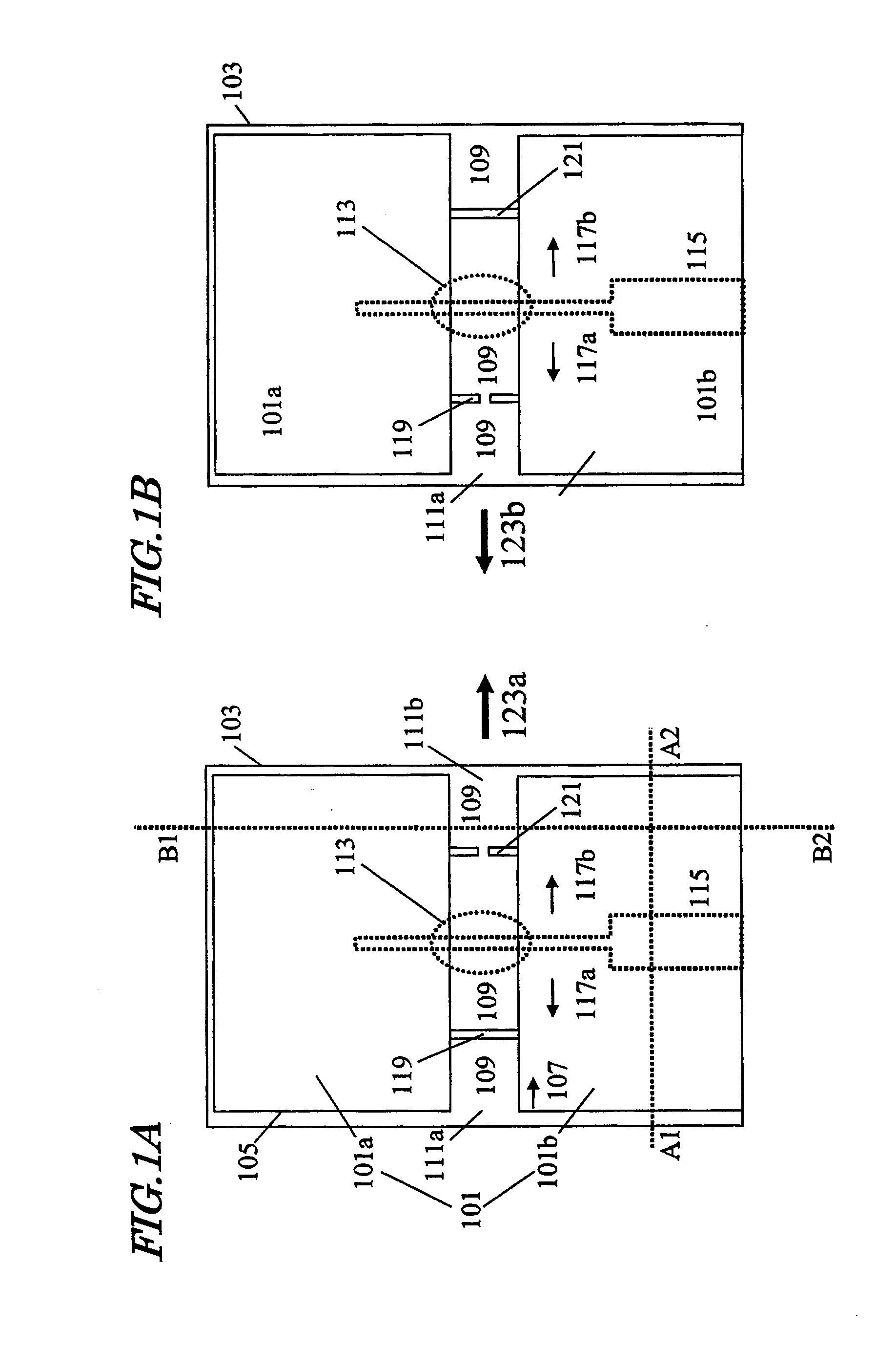
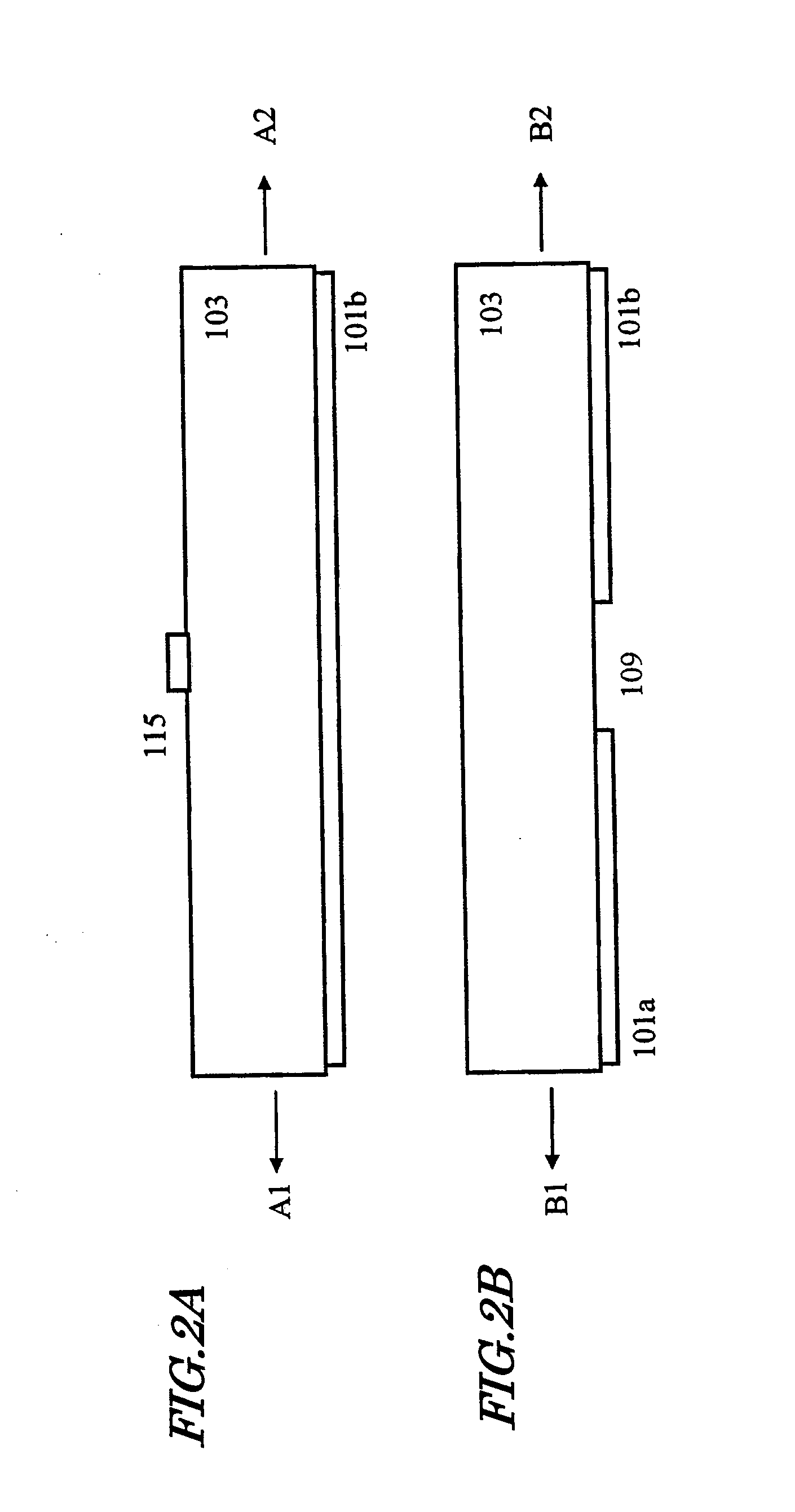
[0055]FIGS. 1A and 1B are lower schematic see-through views (see-through views as seen through the rear face) showing the structure of a variable slot antenna to be driven by a driving method according to the present embodiment, and schematically illustrate switchability as to directivity characteristics of the variable slot antenna obtained in two states of the present driving method. FIGS. 2A and 2B show schematic cross-sectional views of the structure taken along lines A1-A2 and B1-B2 in FIGS. 1A and 1B. For simplicity of discussion, a variable slot antenna structure which is symmetric between right and left will be illustrated as an example of a high-symmetry embodiment, and an embodiment of a driving method which involves switching the main beam direction toward the right or left will be described.
[0056]A ground conductor 101 having a finite area is formed on a rear face of a dielectric substrate 103, and a slot region 109 is formed which recesses into the ground conductor 101 ...
example
[0080]A variable slot antenna of Example 1, as shown in a schematic see-through view (through a lower face) of FIG. 14, was produced. As a dielectric substrate 103, an FR4 substrate having an overall thickness of 0.5 mm was used. On the front face and the rear face of the substrate, respectively, a feed line pattern and a ground conductor pattern each having a thickness of 20 microns were formed, by using a copper line. Each wiring pattern was formed by removing some regions of the metal layer through wet etching, and gold plating was provided on the surface to a thickness of 1 micron. The wiring margin was set so that, even at the closest points to the end faces of the dielectric substrate 101, an outer edge 105 of the ground conductor 101 remained inside the dielectric substrate 103 by no less than 0.1 mm from the end faces. In the figure, the ground conductor pattern is shown by a solid line, whereas the feed line pattern is shown by a dotted line. A high-frequency connector was ...
PUM
 Abstract
Description
Claims
Application Information