

Nonvolatile Semiconductor Storage Device and Method for Writing Therein
a storage device and nonvolatile technology, applied in semiconductor devices, digital storage, instruments, etc., can solve the problems of said difficulty in realizing gate lengths of 130 nm for memory cells of nor type flash memory, and achieve the effect of reducing the potential difference, reducing the number of voltage stepping-up circuits to generate voltage in the chip, and scaling the chip area
- Summary
- Abstract
- Description
- Claims
- Application Information
AI Technical Summary
Benefits of technology
Problems solved by technology
Method used
Image

Examples
Embodiment Construction
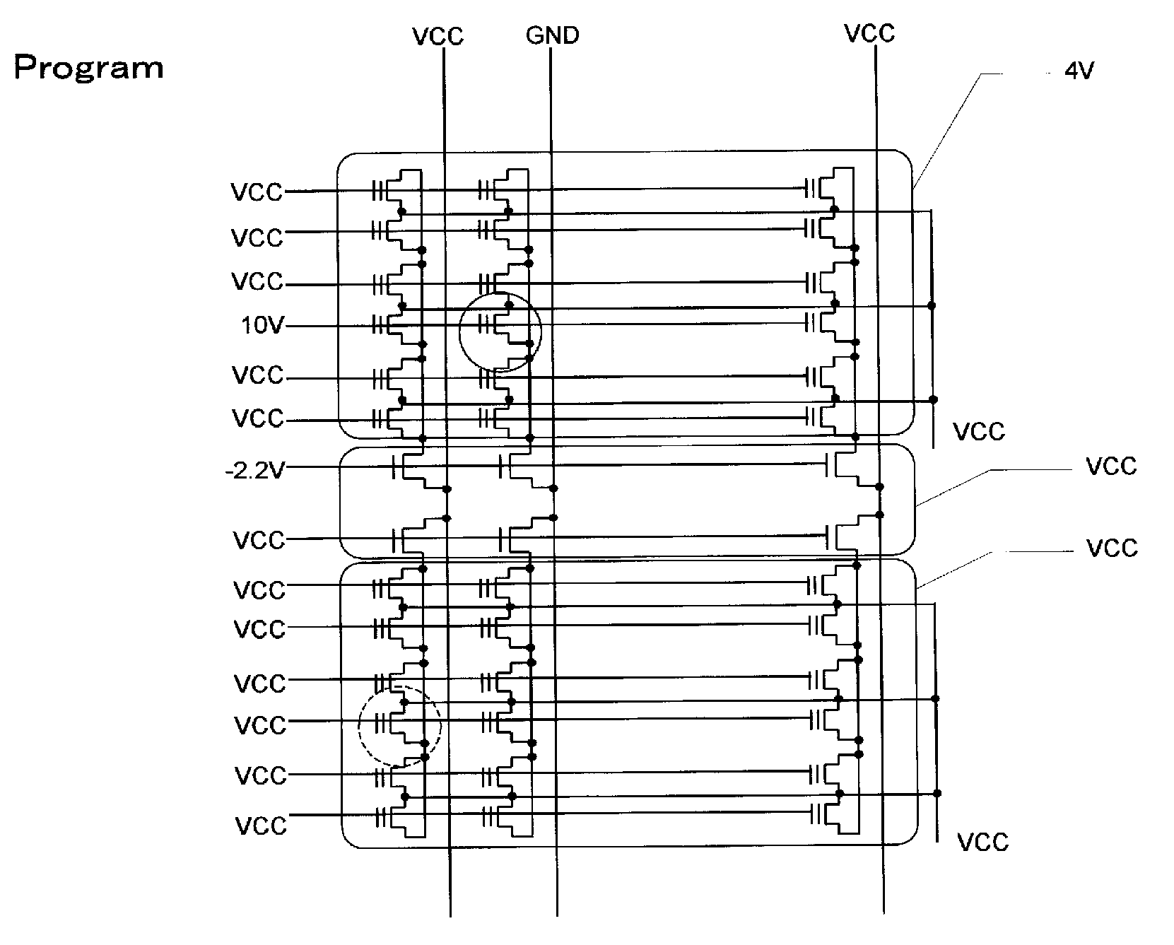
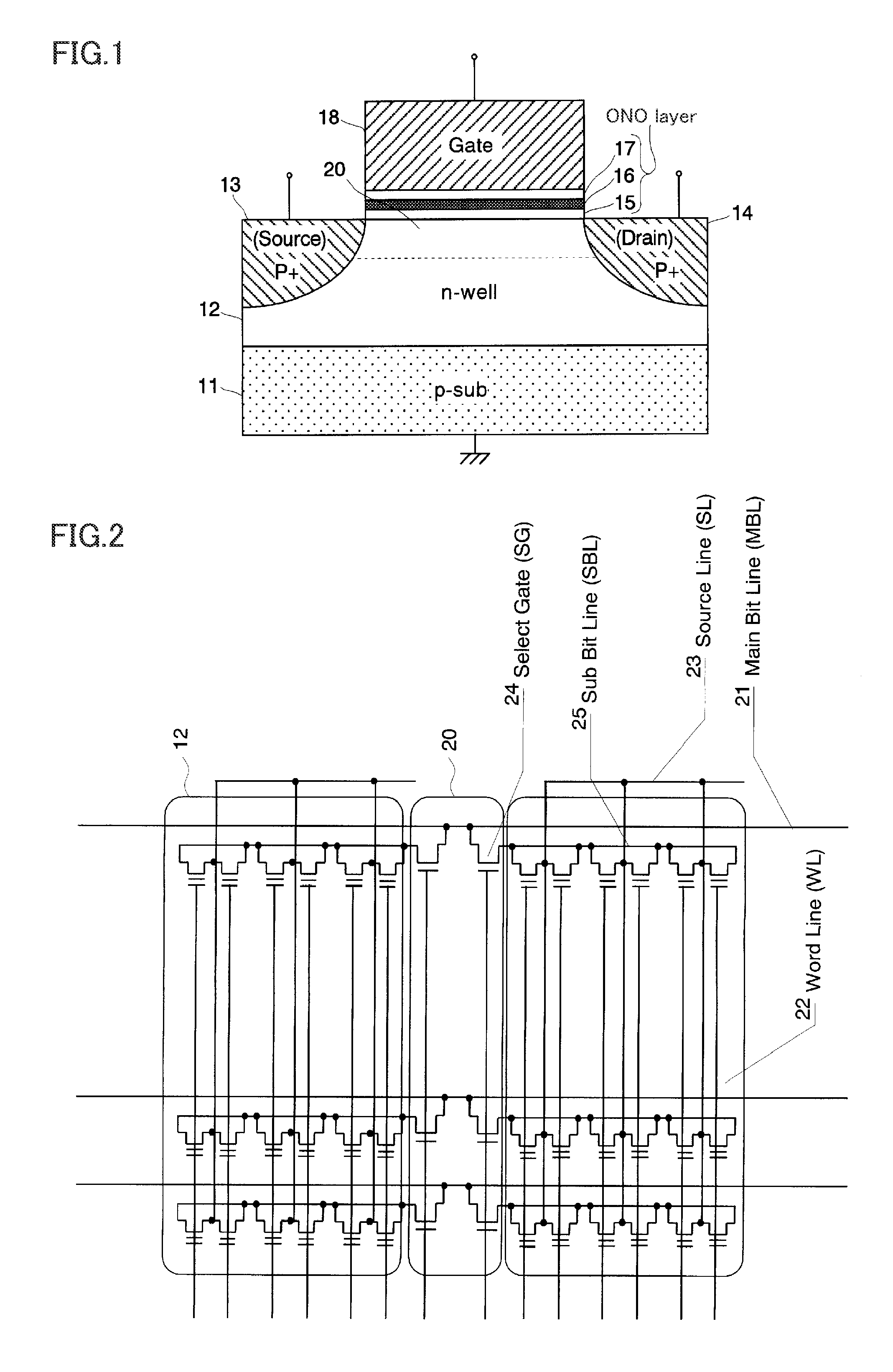
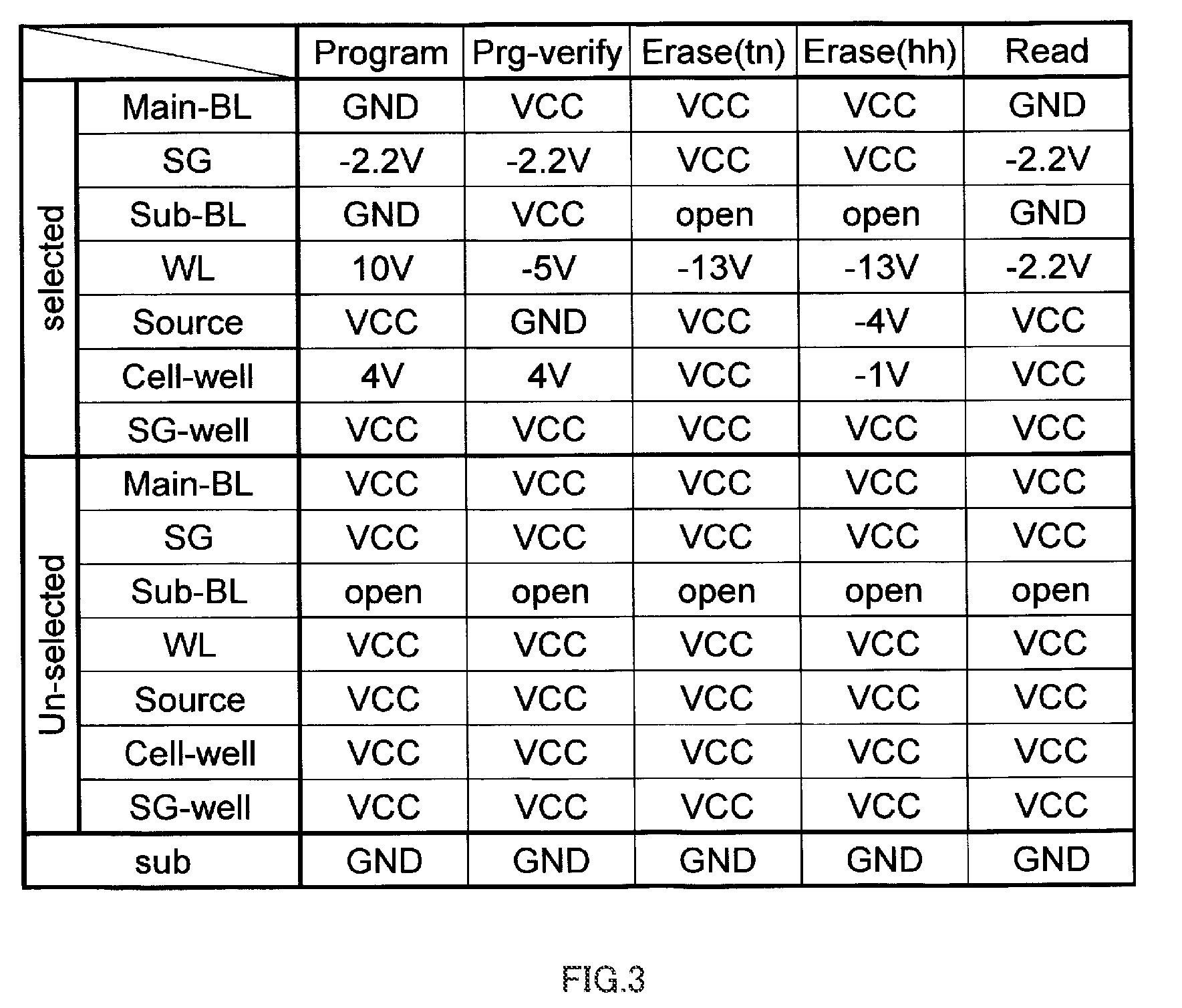
[0068]The embodiments of the invention will be explained with reference to the accompanying drawings. FIG. 1 shows a schematic configuration of the p-channel MONOS memory cell implementing the present invention. The memory cell has an n type well (cell well) 12 formed in a semiconductor substrate 11, a p+ region (source) 13 and a p+ region (drain) 14 formed near the surface of the n type well with a predetermined interval, a channel region 20 formed between the two p type regions 13 and 14, and an ONO layer and a gate electrode 18 formed above the channel region 20 and to cover the channel region 20.
[0069]The ONO layer consists of a tunnel insulating layer 15 made by silicon oxide, a charge trap layer 16 to accumulate injected charges made by silicon nitride and an insulating layer 17 made by silicon oxide. The thicknesses of these three layers: the thickness of the tunnel insulating layer 15 is approximately 2.5˜5 nm, the thickness of the charge trap layer 16 is approximately 10 nm...
PUM
 Abstract
Description
Claims
Application Information