Method and system for printing aligned nanowires and other electrical devices

Active Publication Date: 2008-11-13
SHARP KK
View PDF33 Cites 45 Cited by
  • Summary
  • Abstract
  • Description
  • Claims
  • Application Information

AI Technical Summary

Benefits of technology

[0016]In another aspect of the present invention, nanostructures, such as nanowires, are transferred to a destination surface. A transfer surface of a print head is positioned adjacent to a destination surface. A nanowire is associated with the transfer surface. A distance between the transfer surface and the destination surface is reduced. A fluid is re

Problems solved by technology

A major impediment to the emergence of this new generation of electronic devices based on nanostructures is the ability to effectively align and deposit the nanostructures on various surfaces, such as substrates.
Electric fields enable the alignment of nanowires suspended in

Method used


Image

  • Method and system for printing aligned nanowires and other electrical devices
  • Method and system for printing aligned nanowires and other electrical devices
  • Method and system for printing aligned nanowires and other electrical devices

Examples


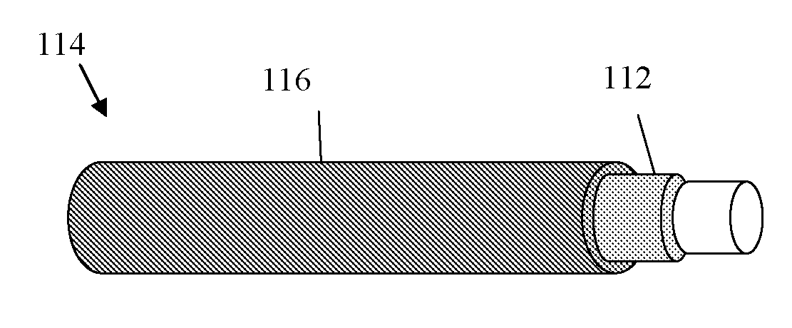
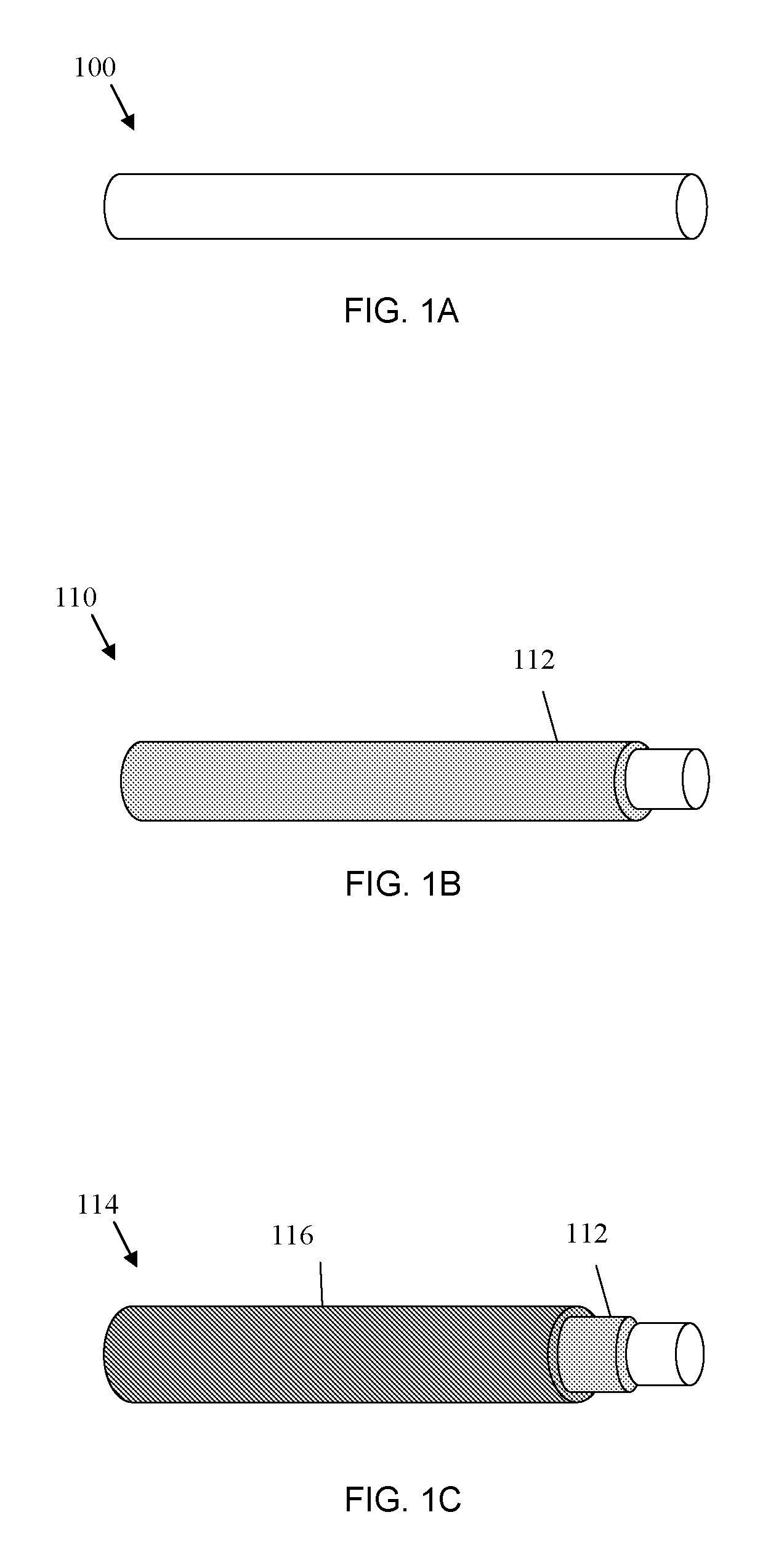
example electrode embodiments

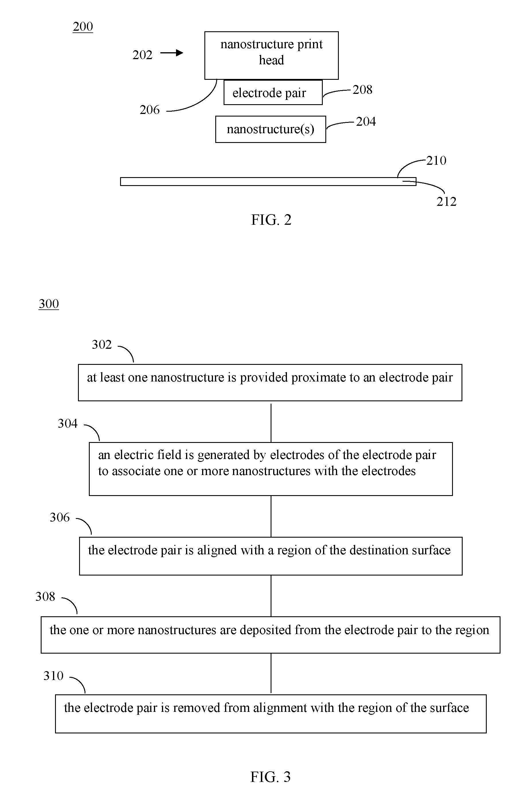
[0191]Nanostructures and / or contaminants may become attached to transfer surfaces of print heads, causing degradation in performance. In embodiments, the transfer surface of nanostructure print heads may be treated to prevent contaminants from sticking, and / to increase a durability of the transfer surface. Such embodiments may be particularly useful to extend a lifetime of a print head / transfer surface when print heads / transfer surfaces are expensive to replace. For example, a coating may be applied to the transfer surface, such as a coating of a non-stick material. In an embodiment, the coating may be removable. In this manner, the coating may be removed and reapplied as needed when a coating wears out, rather than having to dispose of the print head completely.

[0192]For instance, FIG. 47 shows a cross-sectional view of a print head 4700, according to an example embodiment of the present invention. As shown in FIG. 47, a non-stick material layer 4702 is formed on transfer surface 2...


PUM


Abstract

Methods and systems for applying nanowires and electrical devices to surfaces are described. In a first aspect, at least one nanowire is provided proximate to an electrode pair. An electric field is generated by electrodes of the electrode pair to associate the at least one nanowire with the electrodes. The electrode pair is aligned with a region of the destination surface. The at least one nanowire is deposited from the electrode pair to the region. In another aspect, a plurality of electrical devices is provided proximate to an electrode pair. An electric field is generated by electrodes of the electrode pair to associate an electrical device of the plurality of electrical devices with the electrodes. The electrode pair is aligned with a region of the destination surface. The electrical device is deposited from the electrode pair to the region.

Description

[0001]This application claims the benefit of U.S. Provisional Application No. 60 / 916,337, filed on May 7, 2007, which is incorporated by reference herein in its entirety.BACKGROUND OF THE INVENTION[0002]1. Field of the Invention[0003]The present invention relates to nanostructures, and more particularly, to the deposition of aligned nanostructures and electrical devices.[0004]2. Background of the Invention[0005]Nanostructures, such as nanowires, have the potential to facilitate a whole new generation of electronic devices. A major impediment to the emergence of this new generation of electronic devices based on nanostructures is the ability to effectively align and deposit the nanostructures on various surfaces, such as substrates. Electric fields enable the alignment of nanowires suspended in suspension, but current techniques pose stringent constraints on the scalability to large area substrates. Likewise, current techniques for depositing electrical devices, such as integrated ci...

Claims


Application Information

Patent Timeline
IPC IPC(8): B05B5/025H01T14/00
CPCB82B3/00B82Y40/00B82Y30/00H01L21/6835H01L2221/68354H01L2221/68363H01L21/82
Inventor PARCE, J. WALLACEHAMILTON, JAMES M.MARTIN, SAMUELFREER, ERIK
Owner SHARP KK
Why Eureka
Try Eureka