Circuit and method for a three dimensional non-volatile memory

a non-volatile memory and circuit technology, applied in the field of circuits and methods for providing three-dimensional non-volatile memory cells, can solve the problems of device failure, unpredictable threshold voltage (vt), other deleterious effects, etc., and achieve the effects of high integration, relaxed thermal budget for semiconductor processes, and dense and compact structur

Inactive Publication Date: 2008-11-20
TAIWAN SEMICON MFG CO LTD
View PDF3 Cites 100 Cited by
  • Summary
  • Abstract
  • Description
  • Claims
  • Application Information

AI Technical Summary

Benefits of technology

[0009]In another preferred embodiment, a SONOS cell is provided as a patterned FD-SOI structure that is uniformly doped to provide the source drain and channel region, and a polysilicon gate structure is formed overlying an ONO dielectric layer. The SONOS storage cell is provided as a uniformly doped region in an SOI layer of silicon over the interlevel dielectric layers, because there are not separate source drain diffusion regions, the cell is not adversely affected by undesirable diffusion as subsequent layers are processed.
[0011]In another preferred embodiment, the non-volatile storage array may be provided as a core of memory cells that is integrated with logic or processor circuitry to provide an application specific integrated circuit (ASIC) or system on a chip (SOC) that is highly integrated. These highly integrated circuits may reduce the component count required to implement important electronic systems functions such as cell phone circuitry, PDAs, laptop or portable computers, music and video players, and the like.

Problems solved by technology

In FIG. 1, the undesired additional thermal diffusion of the source and drain regions is shown, if this undesired diffusion continues over many process steps the two regions may even electrically contact and close the channel region between them, causing device failure.
Even if such a failure does not occur, the source and drain diffusion changes the channel length, and affects the operation of the device after it is completed, resulting in unpredictable threshold voltages (Vt) and other deleterious effects.

Method used


Image

  • Circuit and method for a three dimensional non-volatile memory
  • Circuit and method for a three dimensional non-volatile memory
  • Circuit and method for a three dimensional non-volatile memory

Examples


Embodiment Construction

[0034]The making and using of the presently preferred embodiments are discussed in detail below. It should be appreciated, however, that the present invention provides many applicable inventive concepts that can be embodied in a wide variety of specific contexts. The specific embodiments discussed are merely illustrative of specific ways to make and use the invention, and do not limit the scope of the invention.

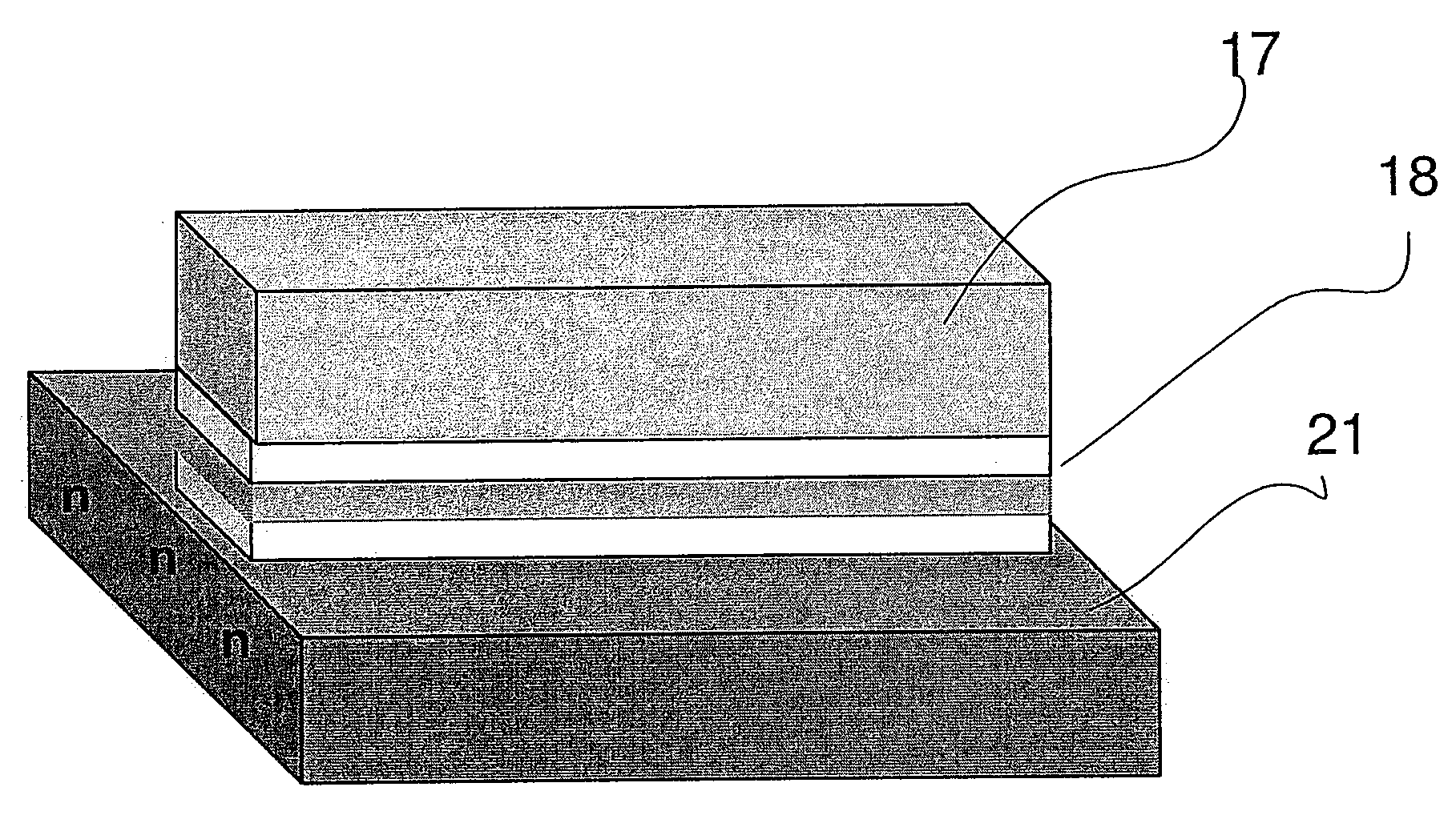
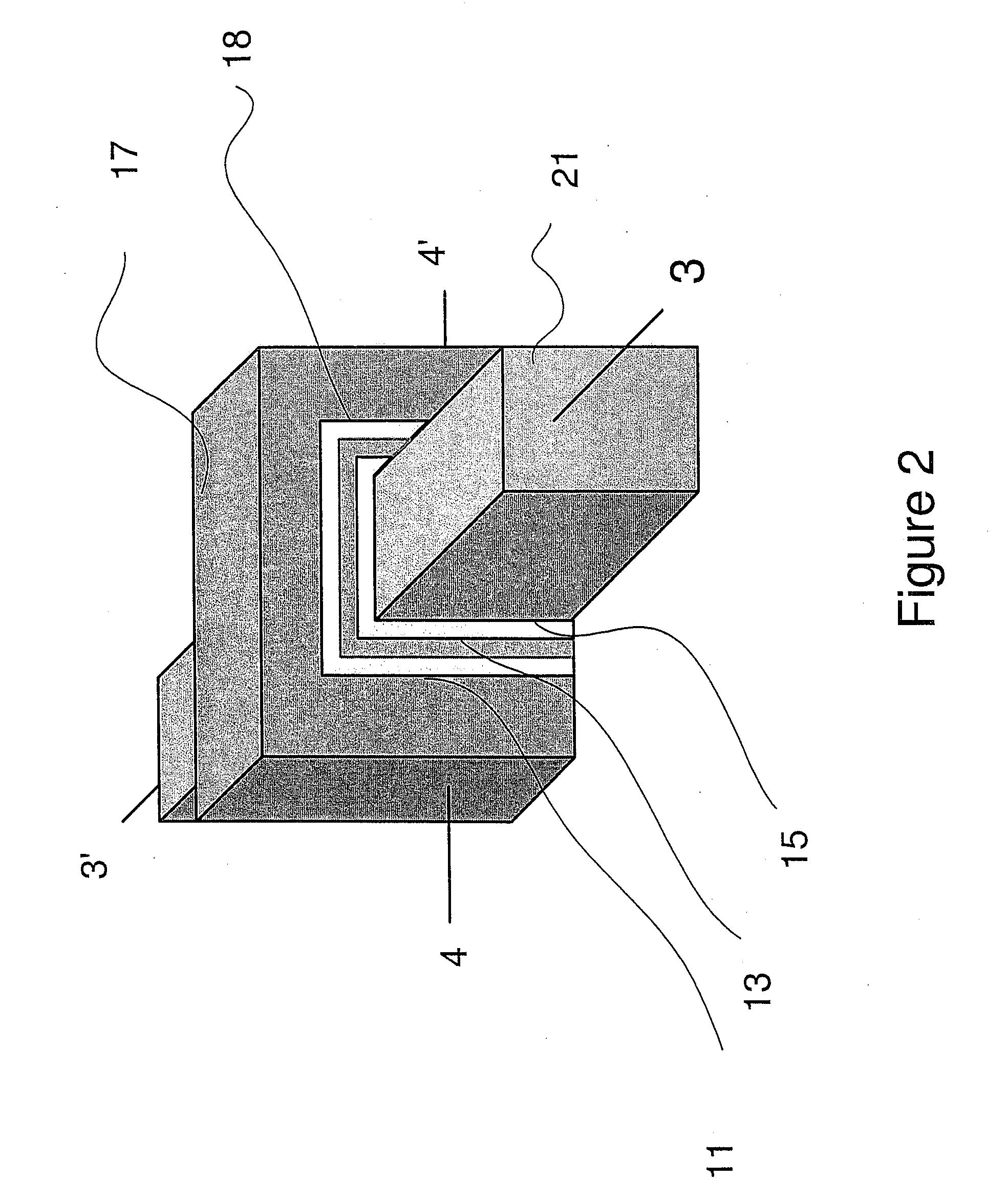
[0035]FIG. 2 depicts in a simple three dimensional view a preferred embodiment of the non-volatile memory cell of the invention. In the preferred embodiment of FIG. 2, the cell is implemented using a FinFET or triple gate MOS transistor approach. A silicon layer 21, typically an epitaxially grown or otherwise deposited polysilicon, is formed and uniformly doped. Alternatives to the polysilicon include bulk silicon, which is doped. The doping is preferentially performed as the polysilicon is deposited or grown, e.g. in situ and in a preferred embodiment, the doping is uniform....


PUM


Abstract

An architecture, circuit and method for providing a very dense, producible, non volatile FLASH memory with SONOS cells. Preferred SONOS memory cells are formed using a uniformly doped channel region. A FinFET embodiment and a planar FD-SOI embodiment cell are disclosed. Because the novel SONOS cells do not rely on diffused regions, the cells may be formed into a three dimensional array of cells without diffusion problems from subsequent thermal processing steps. FLASH memory arrays are formed by forming layers of NAND Flash cells in the local interconnect layers of an integrated circuit, with the metal layers forming the global bit line conductors. The three dimensional non volatile arrays formed of the SONOS cells rely on conventional semiconductor processing and so are easily integrated with other circuitry to form an ASIC or SoC device. P-channel and n-channel devices may be used to form the SONOS non-volatile cells.

Description

TECHNICAL FIELD[0001]The present invention relates to a circuit and method for providing a three dimensional non-volatile memory cell using charge trapping storage in a silicon oxide nitride-oxide ONO silicon (SONOS) flash memory device. The cell incorporates a uniform doping for the source, drain and channel regions. In one preferred embodiment a FinFET form is used another preferred embodiment a fully-depleted silicon on insulator (FD-SOI) form is used. The cell utilizes a charge trapping transistor using ONO or other similar dielectrics. A plurality of these non-volatile memory cells may be arranged in three dimensions using vertical layers. Processing methods are presented for fabricating integrated circuits incorporating memory portions using the SONOS cells. These cells are particularly useful to increase the density of a Flash NAND memory array because the uniform doping in the source, drain and channel circumvents thermal source and drain out diffusion problems that occurred...

Claims


Application Information

Patent Timeline
Patent Type & Authority Applications(United States)
IPC IPC(8): G11C11/34
CPCG11C16/0466H01L27/0688H01L27/115H01L27/11568H01L27/11578H01L29/4234H01L29/66833H01L29/792H10B69/00H10B43/30H10B43/20
Inventor YEH, CHIH CHIEH
Owner TAIWAN SEMICON MFG CO LTD
Why Eureka
Try Eureka