Polyimide-Metal Laminated Body and Polyimide Circuit Board

a technology of polyimide metal and laminated body, which is applied in the direction of insulating substrate metal adhesion improvement, electric connection formation of printed elements, transportation and packaging, etc., can solve the problems of complex manufacturing steps which are combined in a vapor deposition process and wet process in this method, and achieve satisfactory electrical insulating reliability and cohesion. , the effect of satisfactory cohesion

Inactive Publication Date: 2008-11-20
UBE IND LTD
View PDF3 Cites 6 Cited by
  • Summary
  • Abstract
  • Description
  • Claims
  • Application Information

AI Technical Summary

Benefits of technology

[0008]It is therefore an object of the present invention to provide a laminated body and polyimide circuit board that do not require a complex vacuum process, have satisfactory cohesion in wet plating steps, maintain a practical cohesion even after high temperature aging treatment, and exhibit a satisfactory electrical insulating reliability.
[0012]According to the invention, it is possible to obtain a polyimide-metal laminated body and polyimide circuit board which do not require a complicated vacuum process for vapor deposition of the ground metal on the polyimide film, and which have satisfactory cohesion in wet plating steps, maintain practical cohesion even after high temperature aging treatment, and exhibit satisfactory electrical insulating reliability.

Problems solved by technology

However, as the copper foil is roughened in order to improve the cohesion between the copper foil and polyimide, this method has not been satisfactory for achieving high precision and for high-frequency characteristics.
However, the manufacturing steps which are combined in a vapor deposition process and wet process in this method are complicated.
Particularly, when the conductive layer is formed on both sides by a vapor deposition process, any generated gas is virtually unable to escape from the heated polyimide and the quality is thereby reduced.
However, this has been limited to front / back side connection purposes such as blind vias or throughhole vias, as it has been difficult to accomplish film surface plating over the wide areas necessary for circuit formation.
Chemical plating of polyimides is basically difficult, and adequate cohesive strength has not been possible even when the plating is formed by complicated pre-treatment and post-treatment.
In addition, the cohesive strength is often significantly reduced by continuing an aging treatment at high temperature.
These proposals require treatment in a separate step from the polyimide film formation, and therefore the entire fabrication process for the metal foil laminated body is complex and the heat resistance of the formed surface-modified layer is not always sufficient (Japanese Unexamined Patent Publication No. 2003-136632 and Japanese Unexamined Patent Publication No. 2003-200527).
However, while these methods employ common electroless copper plating and yield a satisfactory initial peel strength, there is no mention regarding the behavior of the peel strength in response to a high-temperature aging treatment.
In addition, as control of the linear expansion coefficient of the polyimide film is not considered, it is difficult to maintain dimensional stability when the metal foil laminated body is used as a circuit board material (Japanese Unexamined Patent Publication No. 2000-289167 and Japanese Unexamined Patent Publication No. 2002-64252).
However, the chemical plating catalyst remains between the lines even after circuit formation, thereby impairing the electrical insulating property.

Method used


Image

  • Polyimide-Metal Laminated Body and Polyimide Circuit Board
  • Polyimide-Metal Laminated Body and Polyimide Circuit Board
  • Polyimide-Metal Laminated Body and Polyimide Circuit Board

Examples


reference example 1

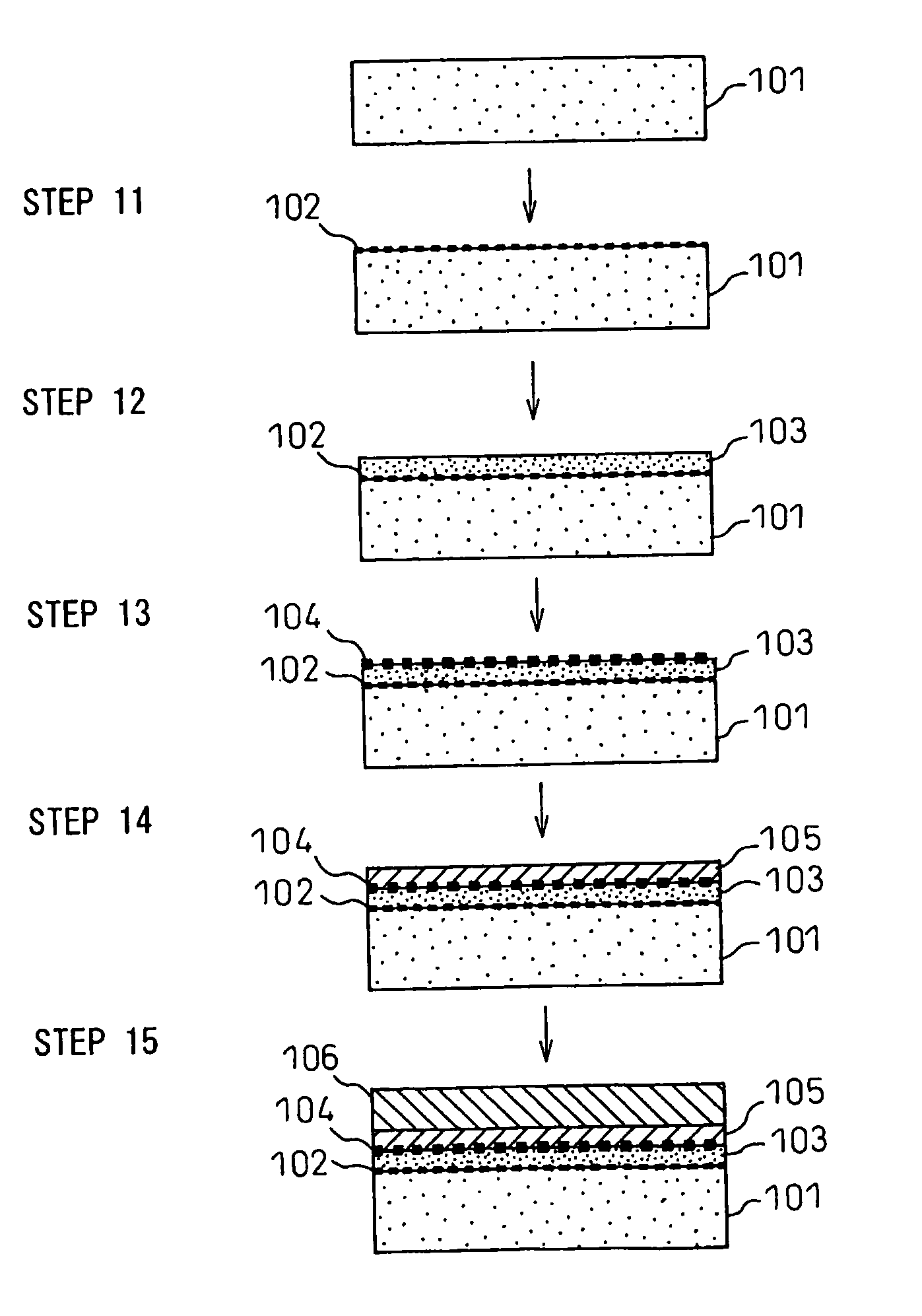
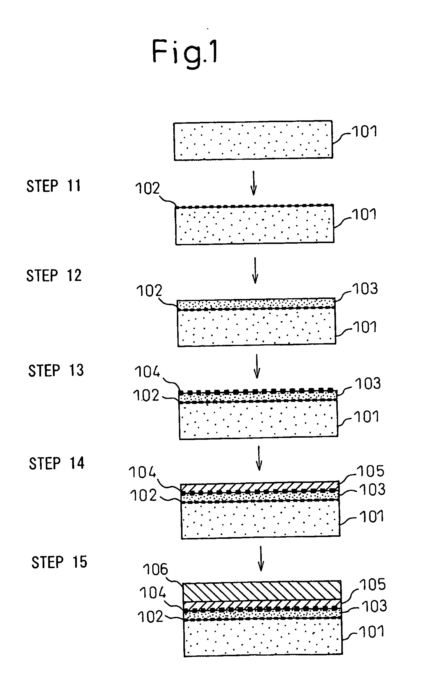
[0054]Fabrication of polyimide film ceramic-modified or pseudoceramic-modified on at least the surface.

[0055]In a 300 ml glass reactor equipped with a stirrer, nitrogen introduction tube and circulation tube there were added 183 g of N,N-dimethylacetamide and 0.1 g of a phosphorus compound (SEPARU 365-100, product of Chukyo Yushi Co., Ltd.), and after further addition of 10.81 g (0.1000 mole) of paraphenylenediamine while stirring under a nitrogen stream, the reactants were heated to 50° C. to complete dissolution. After slowly adding 29.229 g (0.9935 mole) of 3,3′,4,4′-biphenyltetracarboxylic dianhydride while noting the heat release, reaction was continued for 5 hours while maintaining a temperature of 50° C. Next, 0.2381 g (0.00065 mole) of 3,3′,4,4′-biphenyltetracarboxylic dianhydride was dissolved therein. The obtained polyamic acid solution was a brown viscous solution having a solution viscosity of about 1500 poise at 25° C. The thermal expansion coefficient was 15×10−6 cm / cm...

reference example 2

[0057]A polyimide film with a thickness of 25 μm and a silica-modified surface was formed according to the method of Reference Example 1, except that silica gel (a dimethylacetamide solution containing 20 wt % of a silica sol component with a mean particle size of 30 nm, product of Nissan Chemical Industries, Ltd.) and a silane coupling agent (KBM-903, product of Shin-Etsu Chemical Co., Ltd.) were used instead of the aluminum-based coating solution in Reference Example 1, to prepare a dimethylacetamide solution comprising 2.5 wt % of the silica sol component and 0.5 wt % of the silane coupling component, as a coating solution.

example 1

[0058]A ground layer and electroless copper plating layer were accumulated on the polyimide film with a thickness of 25 μm obtained in Reference Example 1 by the plating process shown in Table 1 (“Zintra” process by C. Uyemura & Co., Ltd.). Also, electrolytic copper plating was carried out in a copper sulfate-based electrolytic plating solution for 30 minutes at a current density of 3 A / dm2, and then heat treatment was carried out in a 200° C. oven for 30 minutes to obtain a polyimide copper laminated body with a copper thickness of 10 μm. The results of measuring the 900 peel strength of the obtained polyimide copper laminated body are shown together with the comparative examples in Table 2.

[0059]The results of measuring the 90° peel strength after prolonged aging in an oven with a 150° C. atmosphere are shown in FIG. 5. No deterioration in peel strength was seen even after elapse of 168 hours.

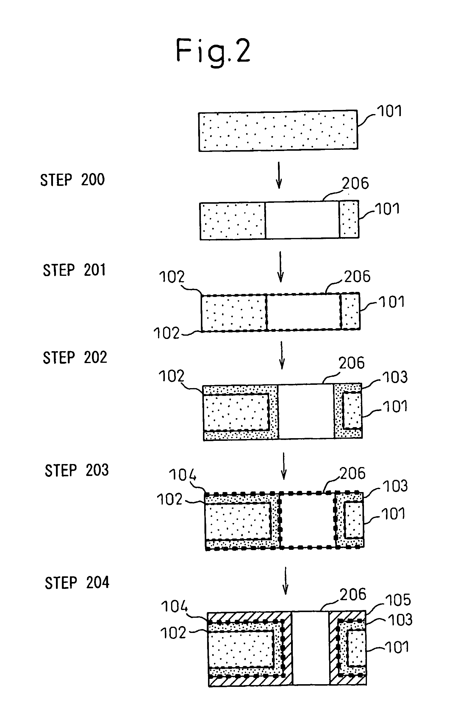
[0060]The obtained laminated body was also used to form a 40 μm pitch comb-shaped electro...


PUM

PropertyMeasurementUnit
RHaaaaaaaaaa
bias voltageaaaaaaaaaa
temperatureaaaaaaaaaa

Abstract

A polyimide-metal laminated body obtained by forming a metal conductive layer on a polyimide film, which has been ceramic-modified or pseudoceramic-modified on at least the surface, by a wet plating process capable of accomplishing metal plating on ceramic. A polyimide-metal laminated body and polyimide circuit board having satisfactory cohesion in wet plating steps, maintain practical cohesion even after high temperature aging treatment, and exhibiting satisfactory electrical insulating reliability, can be obtained.

Description

TECHNICAL FIELD[0001]The present invention relates to a laminated body and polyimide circuit board comprising a polyimide base material and a metal layer, particularly to a polyimide-metal laminated body and polyimide circuit board having a conductive layer formed on a polyimide film by wet plating and, especially, to a flexible polyimide-metal laminated body and polyimide circuit board.BACKGROUND ART[0002]Conventional polyimide laminated boards have been manufactured by laminating a thermoplastic polyimide on one or both sides of a base polyimide layer and thermocompression bonding a copper foil therewith, or by casting a polyimide precursor onto a copper foil and firing it. However, as the copper foil is roughened in order to improve the cohesion between the copper foil and polyimide, this method has not been satisfactory for achieving high precision and for high-frequency characteristics. In order to solve this problem there have been developed and manufactured laminated bodies h...

Claims


Application Information

Patent Timeline
Patent Type & Authority Applications(United States)
IPC IPC(8): B32B15/08H05K1/03H05K3/18H05K3/38H05K3/42
CPCH05K1/0346H05K3/181H05K3/38Y10T428/24917H05K2201/0154H05K2201/0175H05K3/426Y10T428/31721B32B15/08
Inventor YOKOZAWA, TADAHIROYAMAGUCHI, HIROAKIBANBA, KEITAOKUBO, MASAOOKUBO, SUMIKO
Owner UBE IND LTD
Why Eureka
Try Eureka