Package for Light Emitting Device

a technology of light-emitting devices and packaging, which is applied in the direction of semiconductor devices for light sources, light-emitting devices, lighting and heating apparatus, etc., can solve the problems of reducing the efficiency of light-emitting devices, and reducing the size of peripheral equipment, so as to reduce manufacturing costs and reduce manufacturing costs. , the effect of efficient releas

Active Publication Date: 2008-11-27
SUZHOU LEKIN SEMICON CO LTD
View PDF8 Cites 20 Cited by
  • Summary
  • Abstract
  • Description
  • Claims
  • Application Information

AI Technical Summary

Benefits of technology

[0027]According to the present invention, because heat generated from inside the light emitting device package can be efficiently released, as many high output light emitting devices as possible can be arranged in various forms in a restricted space within the package. Thus, the light emitting device package can be utilized in various ways for light emitt

Problems solved by technology

Especially, LEDs have a tendency to become slimmer as information communication equipment are getting smaller in size, and peripheral equipment, such as resistors, condensers, noise filters, etc., are getting much smaller.
However, the light emitting device package 100 having the aforementioned structure has a problem that if the intensity of current is increased in order to obtain light having a high output, a high temperature heat is generated due to poor heat radiation performance in the package.
In a case where the high temperature heat exists in the package without being radiated, the resistance becomes very high and thus the light efficiency becomes deteriorated.
Further, the prior art light emitting device package 100 has a drawback that because the conductor 170, reflecting cup 160, package body 120 and the like are separated from each other, the heat generated from the LED is not easily transferred to outside due to a high heat resistance of their contact portions.
Further, there is an inconvenience that since only one LED is mounted in the package body 120,

Method used


Image

  • Package for Light Emitting Device
  • Package for Light Emitting Device
  • Package for Light Emitting Device

Examples


Embodiment Construction

]

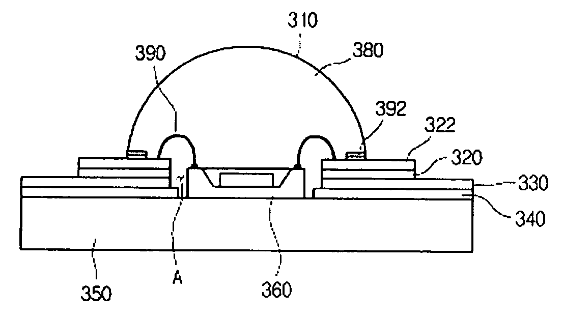
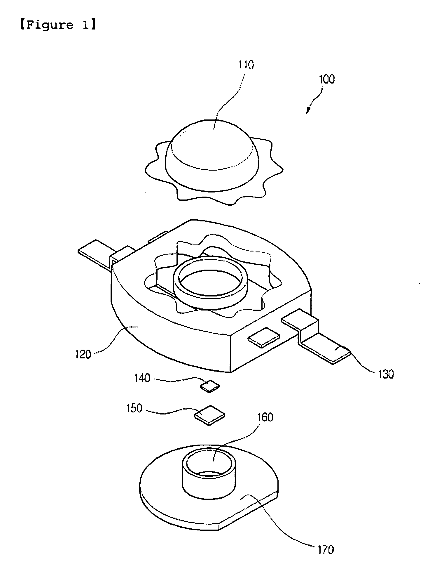
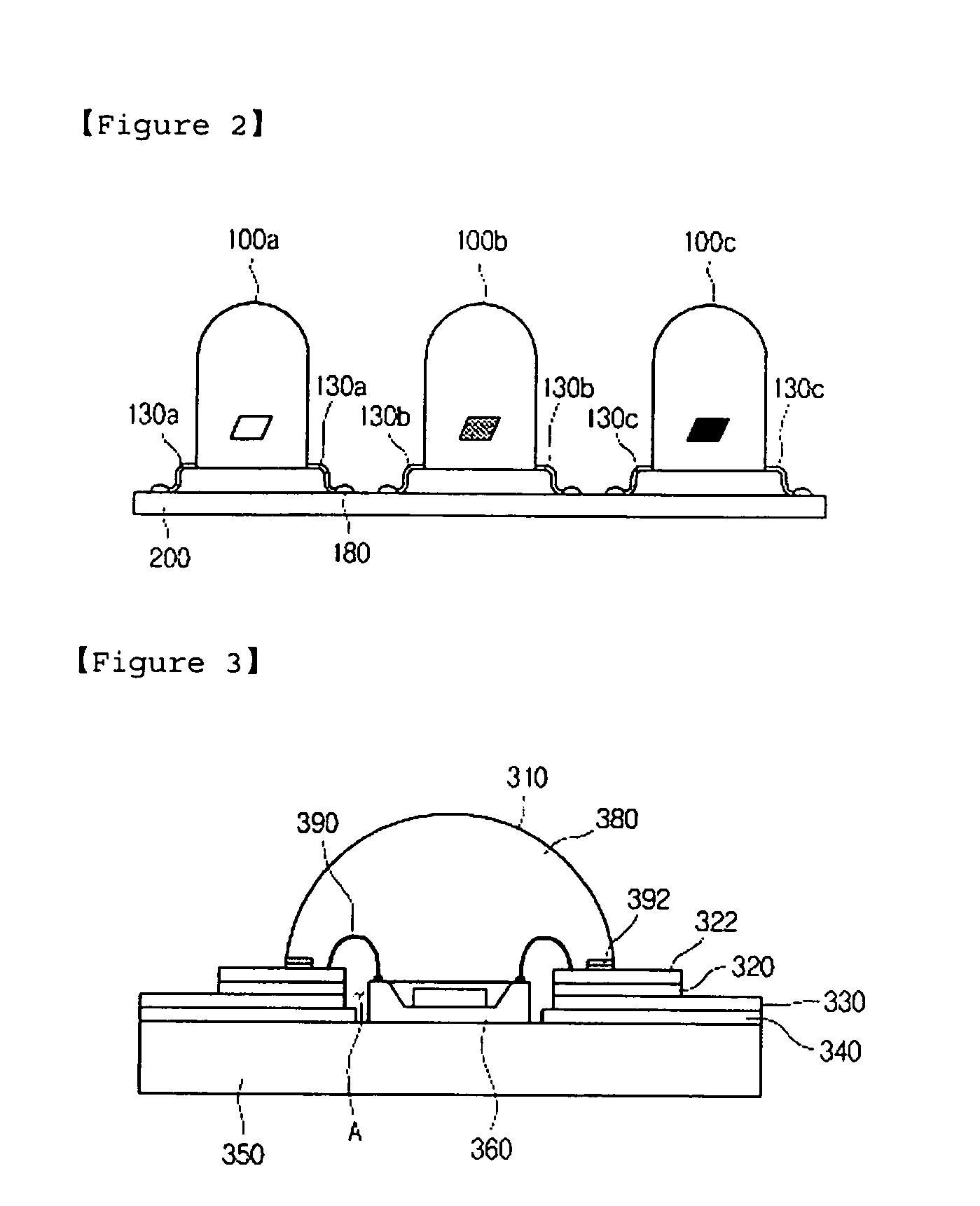
[0075]The light emitting device package according to the present invention proposes a configuration for emitting a high output light, and is primarily focused on an arrangement structure of light emitting devices. To achieve the aforementioned objects, the present invention may be practiced in a variety of embodiments without departing from the foregoing embodiments, and such embodiments may be construed as within the spirit and scope of the present invention.

INDUSTRIAL APPLICABILITY

[0076]According to the light emitting package of the present invention, because heat generated from inside the light emitting device package can be efficiently released, as many high output light emitting devices as possible can be arranged in various forms in a restricted space, and thus, the light emitting device package can be utilized in various ways for products with a tendency to be decreased in size.

[0077]Additionally, according to the present invention, the manufacturing cost can be cut down, an...


PUM


Abstract

The present invention discloses a light emitting device package, comprising: a metal base; an electrical circuit layer provided at an upper side of the metal base for providing a conductive path; a light emitting device mounted in a second region having a smaller thickness than a first region on the metal base; an insulating layer sandwiched between the meta base and the electrical circuit layer; an electrode layer provided at an upper side of the electrical circuit layer; and a wire for electrically connecting the electrode layer and the light emitting device. Further, there is provided a light emitting device package which is improved in light emission efficiency since the light emitting device is placed on a small thickness portion of the metal base.

Description

TECHNICAL FIELD[0001]The present invention relates to a light emitting device package, and more particularly, to a light emitting device package, which is excellent in heat radiation performance and allows circuit design for control of light emission of a semiconductor light emitting device to be freely done.BACKGROUND ART[0002]Generally, as a semiconductor light emitting device, a LED (Light Emitting Diode) can be included, which is a device used for converting electrical signals in the form of infrared, visible and ultraviolet light to emit light by using the characteristics of compound semiconductor.[0003]As for the range of use of LEDs, LEDs are usually used for home appliances, remote controllers, electric signs, displays, a variety of automation equipment, etc, and roughly divided into IRED (Infrared Emitting Diode) and VLED (Visible Light Emitting Diode). The structure of the above-said LED is as follows in general.[0004]Generally, in a blue LED, a N type GaN layer is formed ...

Claims


Application Information

Patent Timeline
IPC IPC(8): H01L33/00H01L33/52H01L33/60H01L33/62H01L33/64
CPCF21K9/00H01L33/52H01L2924/19107H01L2924/0002H01L33/644H01L33/60H01L33/62H01L33/641H01L33/642H05K1/0203H05K1/021H05K1/056H05K1/182H05K3/243H01L33/64Y10S257/918H01L2224/48091H01L2924/00014H01L2924/00H01L33/40H01L33/56H01L33/58H01L27/156H01L33/483H01L33/54H01L2933/0025H01L2933/0058H05K2201/06
Inventor PARK, JUN SEOK
Owner SUZHOU LEKIN SEMICON CO LTD
Why Eureka
Try Eureka