Solid-state imaging device and camera

a solid-state imaging and camera technology, applied in the field of solid-state imaging devices, can solve the problems of low aperture ratio, high reset voltage, and inability to irradiate the backside, and achieve the effects of enhancing sensitivity, reducing reading ability, and increasing distan

Active Publication Date: 2008-11-27
SONY CORP
View PDF7 Cites 108 Cited by
  • Summary
  • Abstract
  • Description
  • Claims
  • Application Information

AI Technical Summary

Benefits of technology

[0021]For the back-irradiation solid-state imaging device disclosed in Patent document 11, hole-accumulating regions are formed on both the front side and back side of the substrate. However, there is a limit to the formation of a shallow heavily-doped p-type semiconductor region through ion-implantation. Therefore, if further increasing of the impurity concentration of the p-type semiconductor region is attempted for dark current suppression, the p-type semiconductor region will range deeper. The deeper p-type semiconductor region leads to larger distance between the p-n junction of the photodiode and the transfer gate, and hence possibly lowers the ability of reading-out by the transfer gate.
[0022]There is a need for the present embodiment to provide a solid-state imaging device and a camera that are allowed to have enhanced sensitivity and miniaturized pixels while efficiently carrying out at high speed a series of operation including generation and accumulation of photo-carriers, charge reading-out, and sending-out of the residual charge (reset), and preventing the deterioration of the sensitivity to blue light and the influence of trapping of photo-carriers at the silicon interface.

Problems solved by technology

Therefore, the backside irradiation is impossible, and the reset voltage is high.
The front-irradiation CMD, BCMD, FWA, and VMIS involve a disadvantage that the aperture ratio is low because a light-receiving part and a pick-up transistor are disposed side by side.
Furthermore, existing photogate structures involve a disadvantage that the sensitivity to blue is low because light is received through a thin film gate.
This leads to a disadvantage that the accumulated carriers are not rapidly discharged when the reset voltage is applied and thus device characteristics are adversely affected.

Method used


Image

  • Solid-state imaging device and camera
  • Solid-state imaging device and camera
  • Solid-state imaging device and camera

Examples


first embodiment

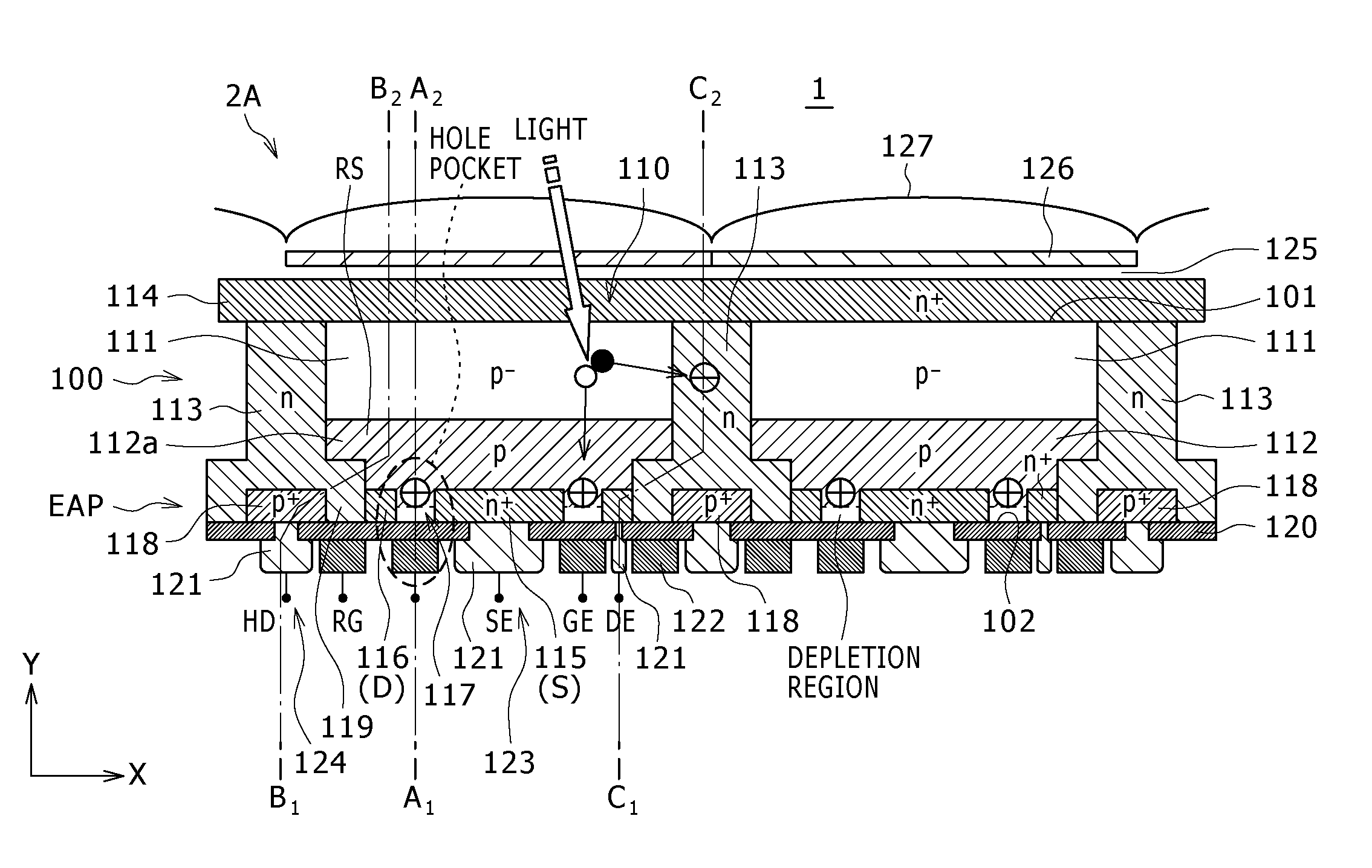
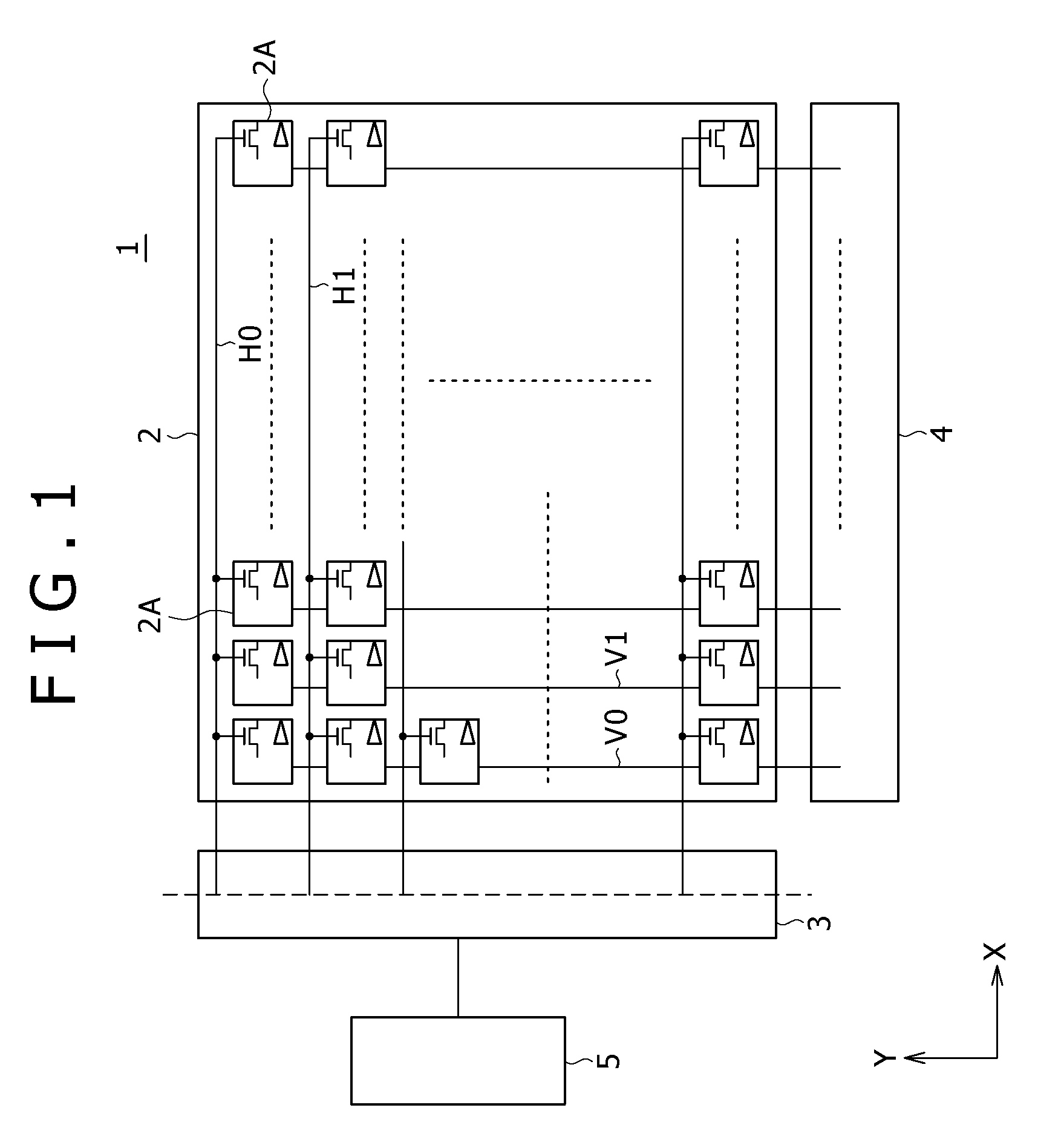
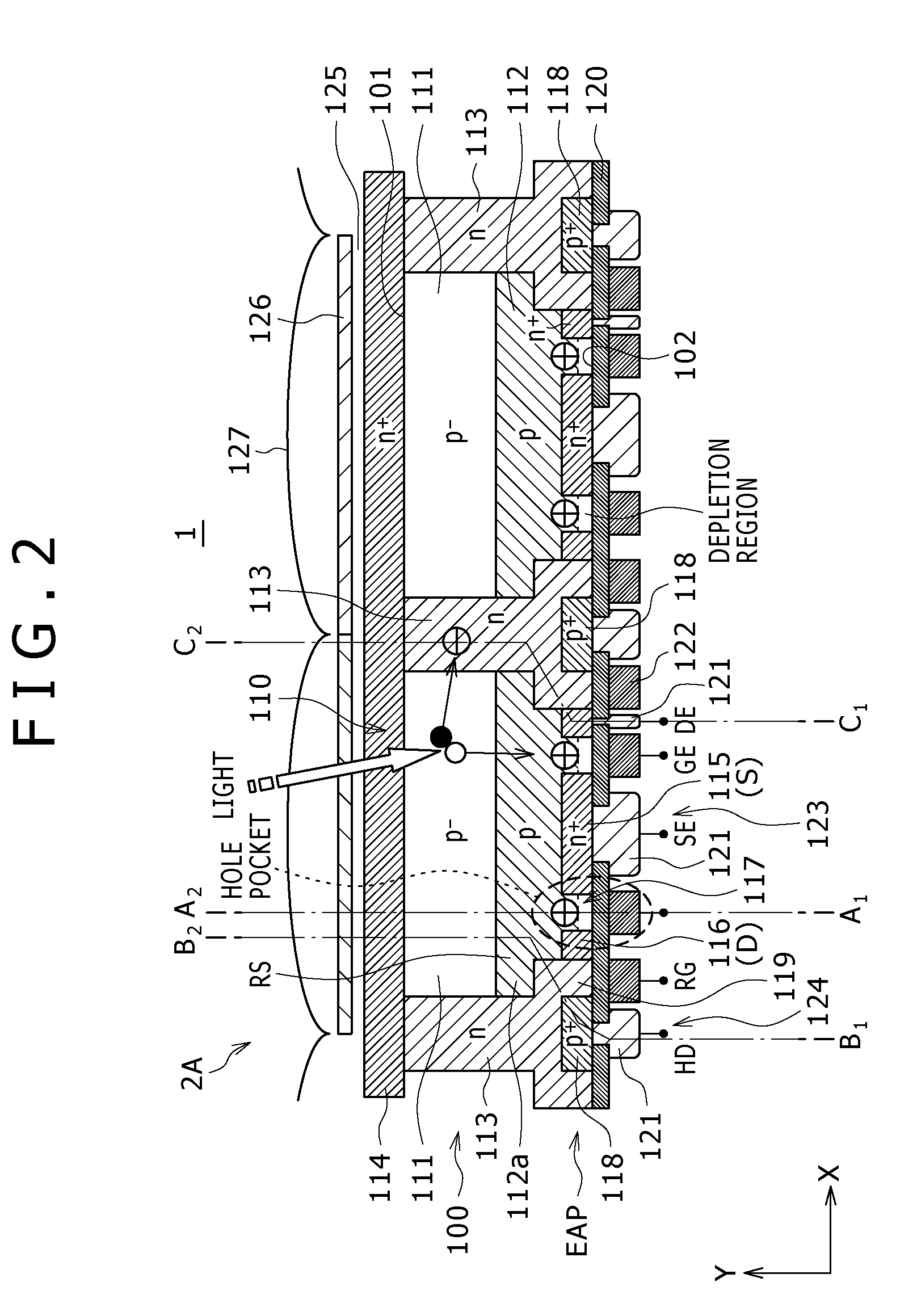
[0053]FIG. 1 is a schematic diagram showing the configuration of a solid-state imaging device according to a first embodiment of the present invention.

[0054]A solid-state imaging device 1 shown in FIG. 1 includes a pixel part 2 as a sensing part, a column-direction (Y-direction) control circuit 3, a row-direction (X-direction) control circuit 4, and a timing control circuit 5.

[0055]The pixel part 2 is formed by arranging pixels 2A each including a light-receiving part, a reset transistor, and so on in a matrix (on rows and columns) as described in detail later.

[0056]The pixel part 2 of the present embodiment is formed as a back-irradiation lateral-overflow image sensor based on a charge modulation system. Each pixel 2A in the present embodiment has a floating cell structure.

[0057]In the pixel part 2, the pixels arranged on the same column are connected to a common column line H0, H1, . . . , and the pixels arranged on the same row are connected to a common row line V0, V1, . . . .

[0...


PUM


Abstract

A solid-state imaging device including: a substrate; a light-receiving part; a second-conductivity-type isolation layer; a detection transistor; and a reset transistor.

Description

CROSS REFERENCES TO RELATED APPLICATIONS[0001]The present invention contains subject matter related to Japanese Patent Applications No. 2007-137446 and No. 2007-137447 filed in the Japan Patent Office on May 24, 2007, the entire contents of which being incorporated herein by reference.BACKGROUND OF THE INVENTION[0002]1. Field of the Invention[0003]The present invention relates to a solid-state imaging device having a photoelectric conversion element and a camera.[0004]2. Description of the Related Art[0005]It is known that, in a solid-state imaging device such as a CCD image sensor and a CMOS image sensor, a crystal defect in a photodiode as a photoelectric conversion element of a light-receiving part and the interface state at the interface between the light-receiving part and an insulating film thereon act as a source of dark current.[0006]As a scheme for suppressing the generation of dark current attributed to the interface state, a buried photodiode structure is effective. This ...

Claims


Application Information

Patent Timeline
Patent Type & Authority Applications(United States)
IPC IPC(8): H01L31/113H04N3/14
CPCH01L27/14621H01L27/14627H01L27/1464H01L27/14656H01L27/14679H01L27/1463H04N25/63H04N25/76
Inventor HIROTA, ISAO
Owner SONY CORP
Why Eureka
Try Eureka