Protective structure

a protective structure and protective technology, applied in the direction of diodes, semiconductor devices, electrical equipment, etc., can solve the problems of high space requirements, complex structure of esd protective structures, inaccurate producability,

Active Publication Date: 2008-11-27
INFINEON TECH AG
View PDF10 Cites 20 Cited by
  • Summary
  • Abstract
  • Description
  • Claims
  • Application Information

AI Technical Summary

Problems solved by technology

Electrostatic discharges (ESD) can severely damage semiconductor components.
Known ESD protective structures have structures that are complicated and have inaccurate producability on account of the high substrate thickness for the diode arrangement.
The dopant diffusion through the complete substrate thickness leads to inaccuracies and a high space requirement owing to the lateral outdiffusion that likewise takes place.
The high substrate thickness brings about a high resistance, which adversely affects the performance of the protective structure.

Method used


Image

  • Protective structure
  • Protective structure
  • Protective structure

Examples


Embodiment Construction

[0010]The present invention specifies a cost-effective method for producing a protective structure having a high performance.

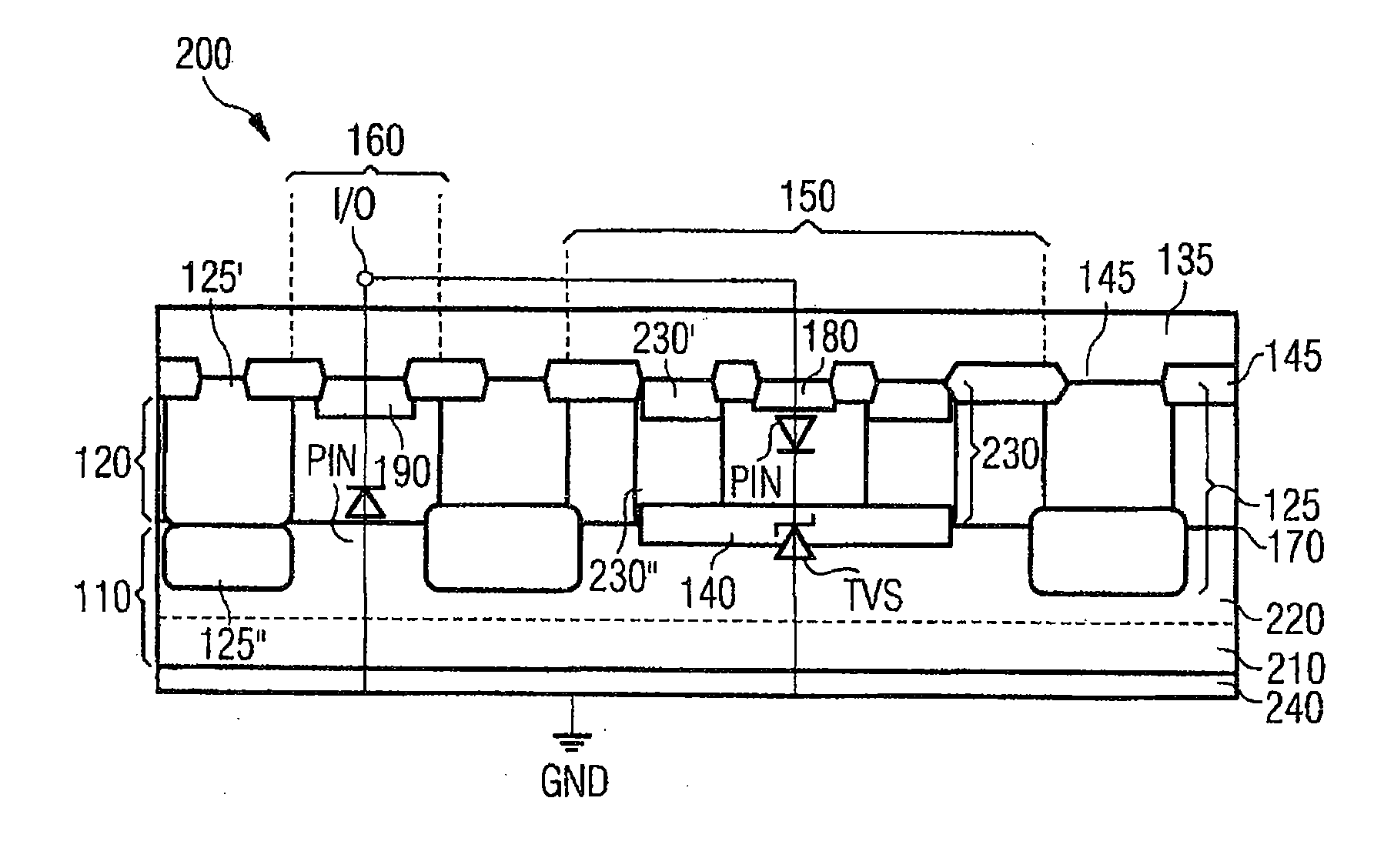
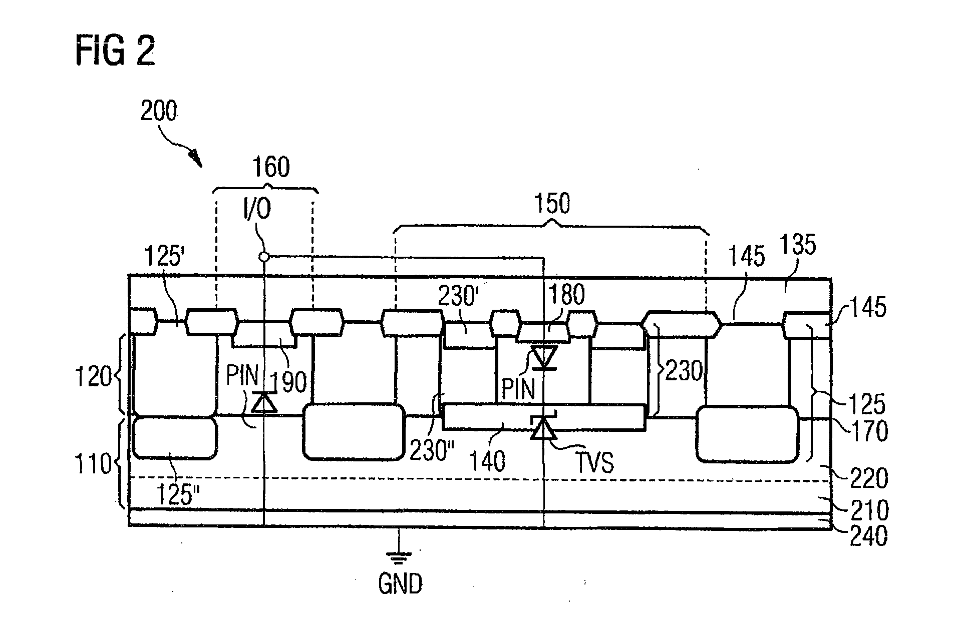
[0011]Embodiments of the invention generally relate to a method for producing a protective structure which involves providing a semiconductor substrate with a doping of a first conductivity type, applying a semiconductor layer with a doping of a second conductivity type at a surface of the semiconductor substrate, forming a buried layer with a doping of a second conductivity type in a first region of the semiconductor layer, wherein the buried layer is produced at the junction between the semiconductor layer and the semiconductor substrate, forming a first dopant zone with a doping of a first conductivity type in the first region of the semiconductor layer above the buried layer, forming a second dopant zone with a doping of a second conductivity type in a second region of the semiconductor layer, forming an electrical insulation between the first region and t...


PUM


Abstract

A protective structure is produced by providing a semiconductor substrate with a doping of a first conductivity type. A semiconductor layer with a doping of a second conductivity type is applied at a surface of the semiconductor substrate. A buried layer with doping of a second conductivity type is formed in a first region of the semiconductor layer, wherein the buried layer is produced at the junction between the semiconductor layer and semiconductor substrate. A first dopant zone with a doping of a first conductivity type is formed in the first region of the semiconductor layer above the buried layer. A second dopant zone with a doping of a second conductivity type is formed in a second region of the semiconductor layer. An electrical insulation is formed between the first region and the second region of the semiconductor layer. A common connection device is formed for the first dopant zone and the second dopant zone.

Description

CROSS-REFERENCE TO RELATED APPLICATION[0001]This application claims priority to German Patent Application Serial No. DE 10 2007 024 355.5, which was filed May 24, 2007, and is incorporated herein by reference in its entirety.FIELD OF THE INVENTION[0002]Exemplary embodiments of the invention relate to a method for producing a protective structure, and the protective structure.BACKGROUND OF THE INVENTION[0003]Electrostatic discharges (ESD) can severely damage semiconductor components. Therefore, ESD protective concepts are realized in most semiconductor components nowadays. The ESD protective components integrated in the chip define a current path via which the ESD current can flow without causing damage.[0004]In the case of high-speed data transmission lines, in particular, the requirement exists of ensuring an ESD protection up to 15 kV without the signal waveform being distorted to an excessively great extent. For this purpose, the protective element must have a particularly low ca...

Claims


Application Information

Patent Timeline
Patent Type & Authority Applications(United States)
IPC IPC(8): H01L21/265H01L29/868
CPCH01L27/0255H01L29/66121H01L21/265H01L21/22H01L29/868Y02E10/548
Inventor SCHMENN, ANDRESOJKA, DAMIANAHRENS, CARSTEN
Owner INFINEON TECH AG
Why Eureka
Try Eureka