Contact made of ceramic and its manufacturing method

a technology of contact and ceramics, applied in the field of contact, can solve the problems of permanent deformation and yield of contact, adverse effect of magnetic field, and magnetic field formation

Inactive Publication Date: 2008-11-27
ALPS ALPINE CO LTD
View PDF1 Cites 8 Cited by
  • Summary
  • Abstract
  • Description
  • Claims
  • Application Information

AI Technical Summary

Benefits of technology

[0012]Thus, the invention has been made in view of these points, and the object of the invention is to provide a contact and its manufacturing method capable of preventing the contact from yielding even if a conduction test of a semiconductor device is repeatedly performed, and capable of suppressing that an adverse effect of a magnetic field is exerted on the semiconductor device.

Problems solved by technology

Thus, sliding deformation of the spring portion 102 at a temperature rise in a conduction test of a semiconductor device (not shown) occurs easily, and if the conduction test is repeatedly performed, there is a problem in that the contact 101 deforms permanently and yields.
Further, since the spring portion 102 is formed using Ni—P that is a magnetic material, there is a problem in that a magnetic field may be formed around the spring portion 102.
Therefore, there is a possibility that an adverse effect of the magnetic field is exerted on a semiconductor device in contact with the contact 101 by the conduction test.

Method used


Image

  • Contact made of ceramic and its manufacturing method
  • Contact made of ceramic and its manufacturing method
  • Contact made of ceramic and its manufacturing method

Examples


first embodiment

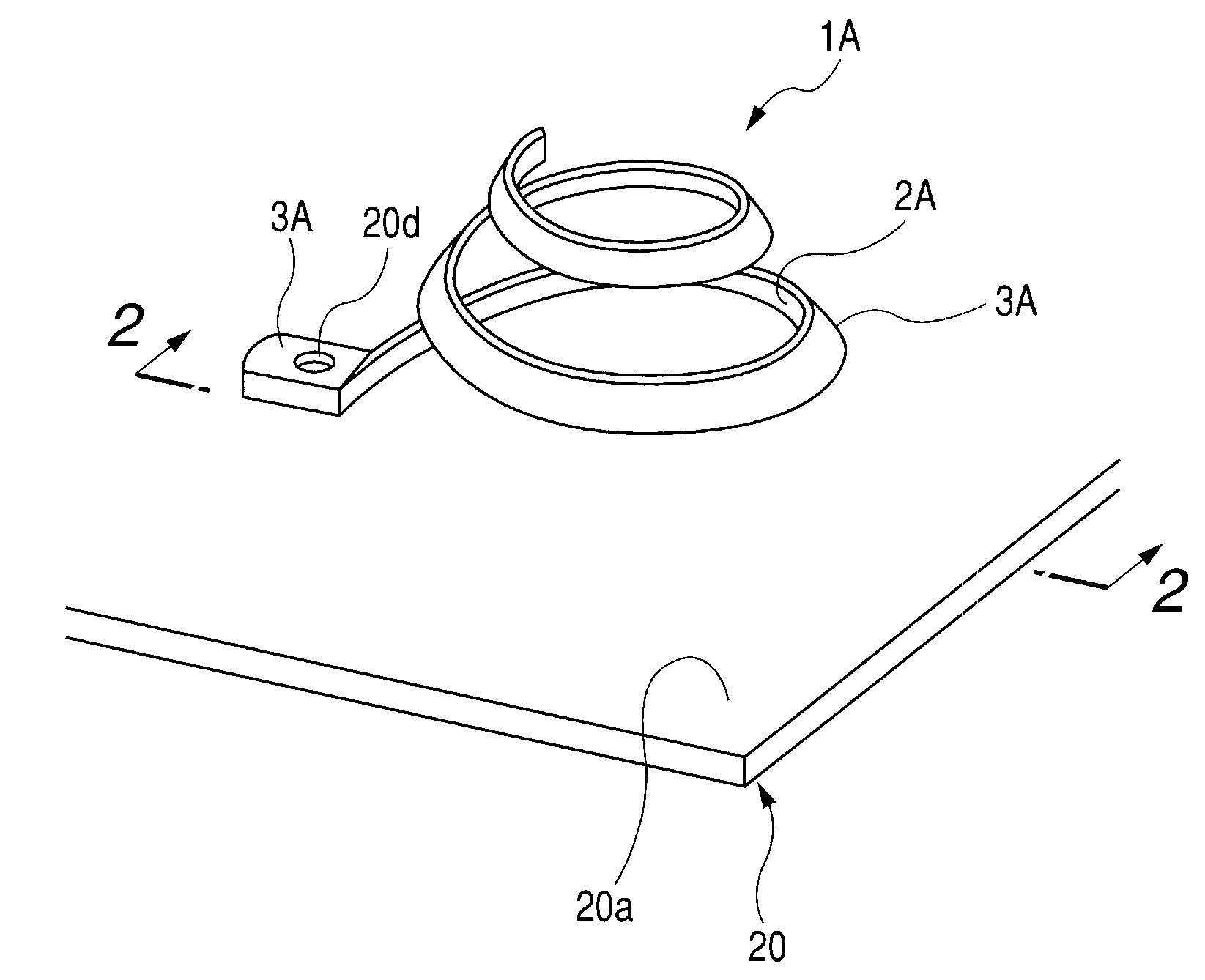
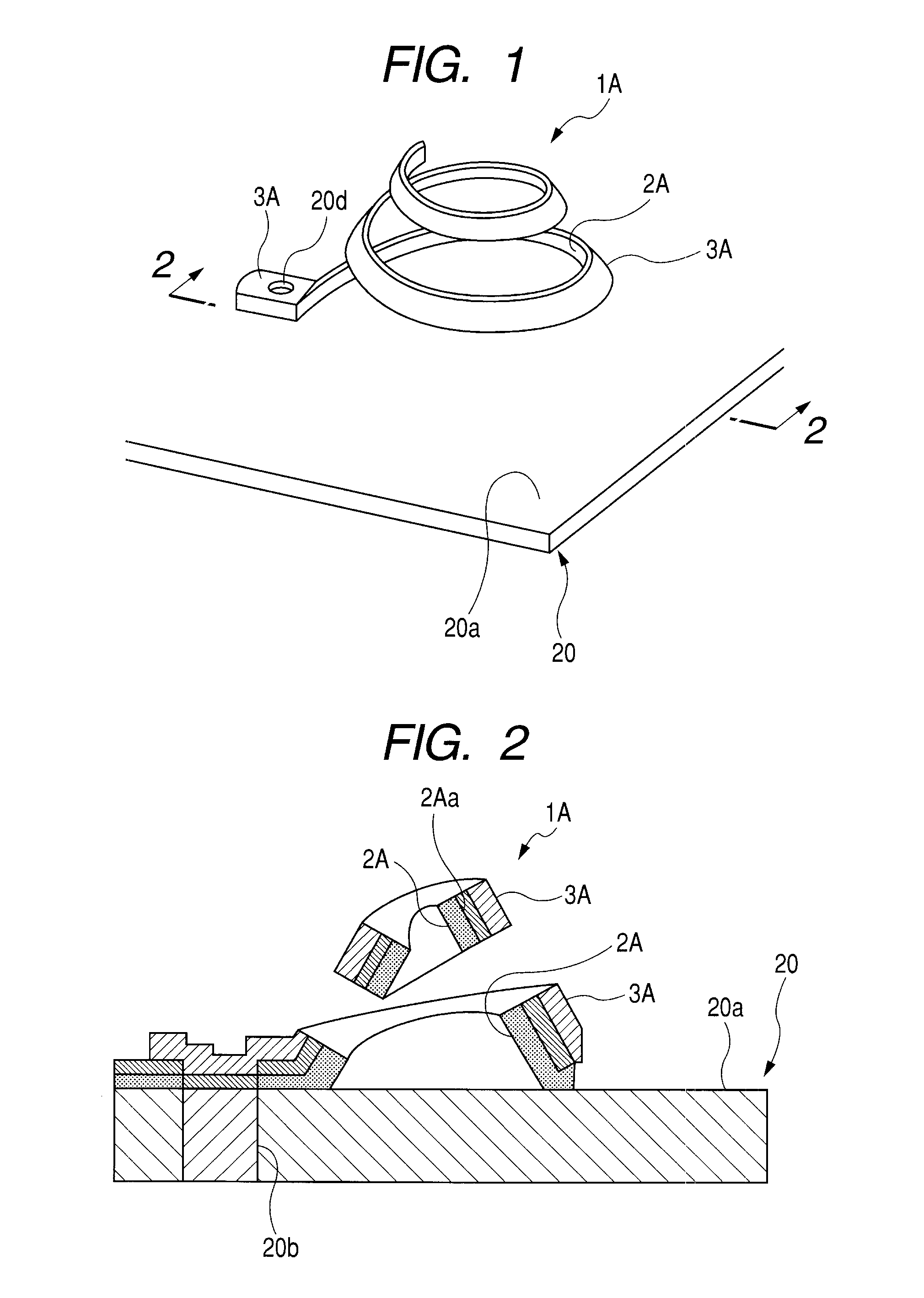
[0067]As shown in FIGS. 1 and 2, the contact 1A of the first embodiment includes a spring portion 2A and a conductive portion 3A.

[0068]The spring portion 2A is formed on the surface of a wiring substrate 20a of a probe card 20, using ceramic. If the shape of the spring portion 2A is the shape of a spring that exhibits an elastic force in a vertical direction, such as a coil spring, a leaf spring, or a disc spring, various shapes can be selected. As the shape of the spring portion 2A of the first embodiment, a convex solid spiral shape that protrudes toward a bump (upper portion of FIG. 2) is selected. In that case, the spring portion 2A is dimensioned such that the diameter thereof is about 200 μm, and the height thereof is about 100 μm.

[0069]Further, the spring portion 2A is formed by an aerosol deposition method capable of forming the spring portion at room temperature. The aerosol deposition method is a film-forming method that mixes ceramic particulates with inert gas within a c...

second embodiment

[0104]As shown in FIG. 5, the contact 1B of the second embodiment includes a spring portion 2B and a conductive portion 3B.

[0105]The spring portion 2B is formed on the surface of the wiring substrate 20a of the probe card 20, using ceramic. The spring portion 2B is the same as that of the first embodiment.

[0106]The conductive portion 3B has a surface-side conductive portion 7B that covers a surface 2Ba of the spring portion 2B that faces the bump using a conductive material, and a back-side conductive portion 8B that covers a back 2Bb. Further, the surface-side conductive portion 7B and the back-side conductive portion 8B are electrically connected as they are formed continuously. That is, the second embodiment is different from the first embodiment in that the conductive portion 3B is formed even on the back 2Bb of the spring portion 2B. The conductive material used for the surface-side conductive portion 7B and the back-side conductive portion 8B mainly includes metals, such as Cu...

third embodiment

[0132]As shown in FIG. 7, the contact 1C of the third embodiment includes a spring portion 2C and a conductive portion 3C.

[0133]The spring portion 2C is formed on the surface of the wiring substrate 20a of the probe card 20, using ceramic. The third embodiment is different from the first embodiment and second embodiment in that the spring portion 2C is formed by sputtering and sintering ceramic. As the ceramic, zirconia-based ceramic, particularly, stabilized zirconia is selected. This point is the same as that of the first embodiment and second embodiment.

[0134]The conductive portion 3C has a surface-side conductive portion 7C that covers a surface 2Ca of the spring portion 2C that faces the bump, and a back-side conductive portion 8C that covers a back 2Cb. Further, the surface-side conductive portion 7C and the back-side conductive portion 8C are electrically connected as they are formed so as to contact each other. The conductive portion 3C is the same as that of the second embo...


PUM

PropertyMeasurementUnit
heightaaaaaaaaaa
heightaaaaaaaaaa
thicknessaaaaaaaaaa

Abstract

A contact of the invention includes a spring portion and a conductive portion. The spring portion is formed on the surface of a wiring substrate of a probe card, using ceramic. The conductive portion is formed thinly so as to cover at least the surface of the spring portion that faces the bump. Thus, as one of the features of a manufacturing method of the contact, the spring portion is formed at room temperature by an aerosol deposition method.

Description

[0001]This application claims benefit of Japanese Patent Application No. 2007-057088 filed on Mar. 7, 2007, which is hereby incorporated by reference.BACKGROUND[0002]1. Field of the Invention[0003]The present invention relates to a contact and its manufacturing method, and specifically, to a contact and its manufacturing method that can be suitably utilized in order to manufacture a spring-type probe (contact) of a probe card that performs electrical connection with a semiconductor device that has a bump (projection electrode) formed in the shape of a ball or land.[0004]2. Description of the Related Art[0005]Generally, in a manufacturing process of a semiconductor device, such as IC (Integrated Circuit) or LSI (Large Scale Integration: IC whose degree of integration of elements is 1000 pieces to 10000 pieces), the vain effort of assembling a poor semiconductor device into a package is reduced by connecting a manufactured semiconductor device to a wiring substrate to be tested called...

Claims


Application Information

Patent Timeline
Patent Type & Authority Applications(United States)
IPC IPC(8): H01R12/22H01R43/16H01R12/71
CPCG01R1/06716G01R3/00H05K3/048H05K3/4092Y10T29/49204H05K2201/10734H05K2203/0588H05K2203/308G01R1/06755H05K2201/0311
Inventor MURATA, SHINJI
Owner ALPS ALPINE CO LTD
Why Eureka
Try Eureka