In-situ STEM sample preparation

Active Publication Date: 2008-12-04
FEI COMPANY
View PDF9 Cites 69 Cited by
  • Summary
  • Abstract
  • Description
  • Claims
  • Application Information

AI Technical Summary

Benefits of technology

[0019]An object of the invention, therefore, is to provide an improved method for STEM sample preparation and analysis that can be used in a FIB-STEM system without a flip stage. Preferred embodiments of the present invention allow a dual beam FIB-STEM system with a typical tilt stage

Problems solved by technology

As features continue to get smaller and smaller, however, there comes a point where the features to be measured are too small for the resolution provided by an ordinary SEM.
Because a sample must be very thin for viewing with transmission electron microscopy (whether TEM or STEM), preparation of the sample can be delicate, time-consuming work.

Method used


Image

  • In-situ STEM sample preparation
  • In-situ STEM sample preparation
  • In-situ STEM sample preparation

Examples


Embodiment Construction

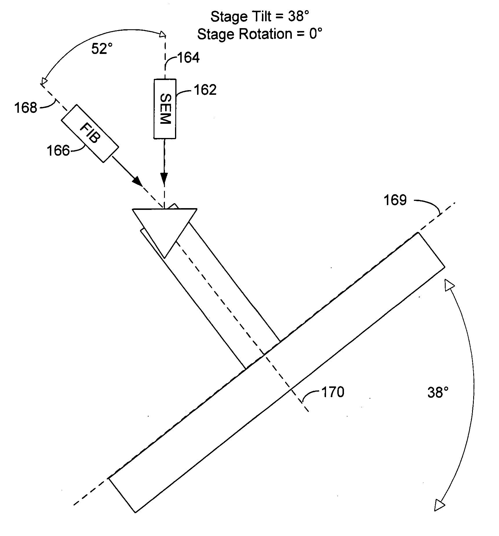
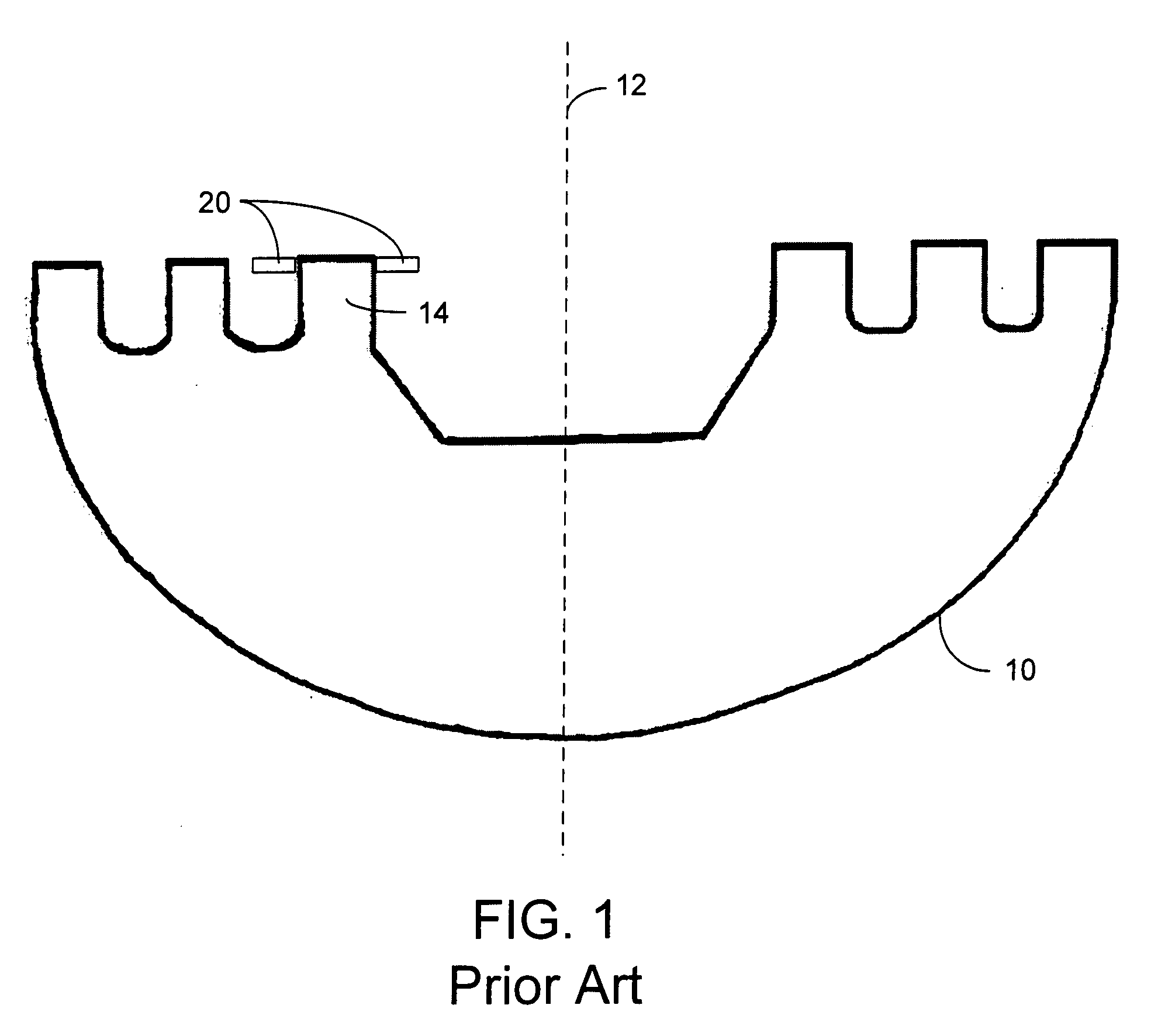
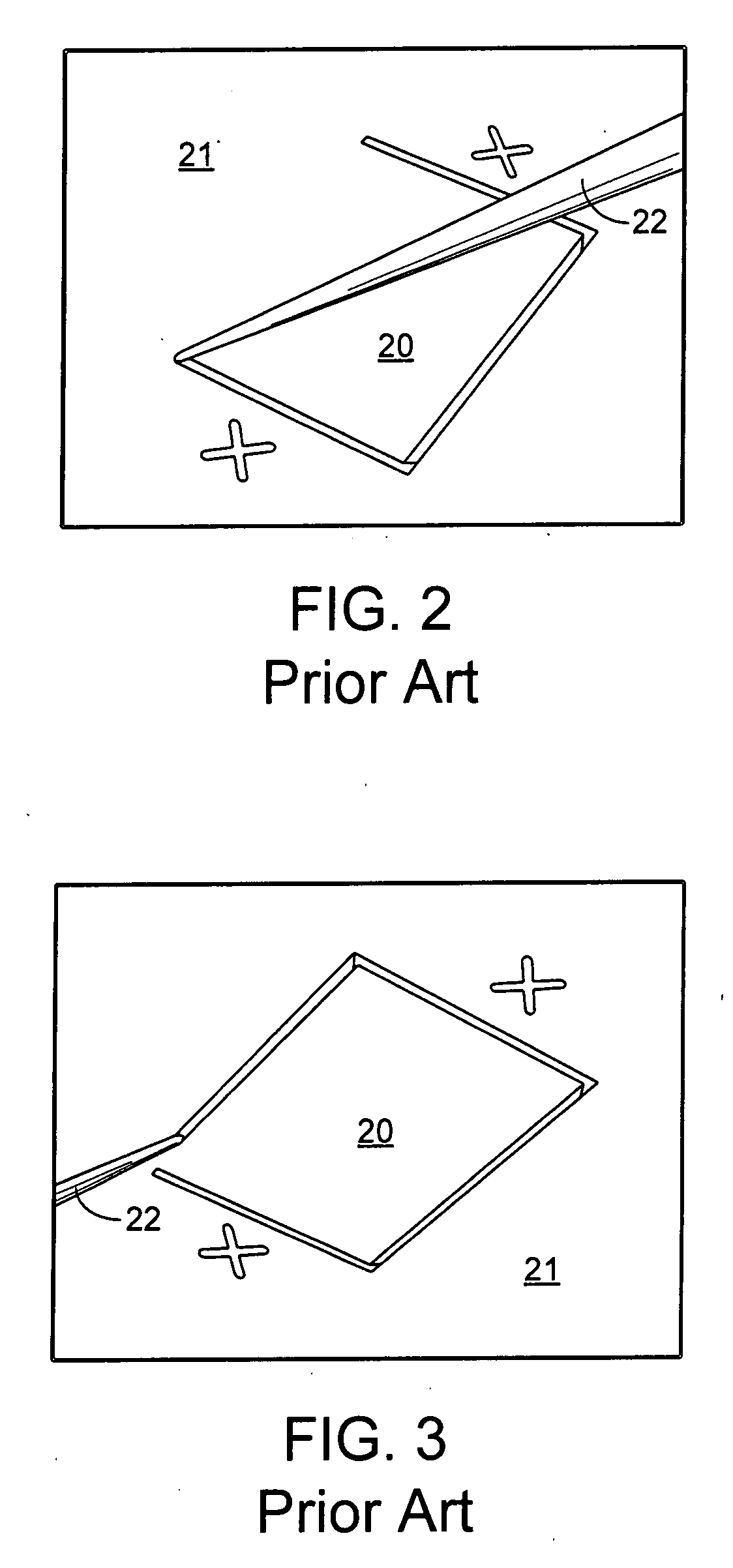
[0033]Preferred embodiments of the present invention provide an improved method for STEM sample preparation and analysis that can be used in a FIB-STEM system without a flip stage.

[0034]A preferred method or apparatus of the present invention has many novel aspects, and because the invention can be embodied in different methods or apparatuses for different purposes, not every aspect need be present in every embodiment. Moreover, many of the aspects of the described embodiments may be separately patentable.

[0035]A preferred method of preparing a sample for STEM imaging according to the present invention comprises the following steps:[0036]providing a substrate inside a dual beam FIB / STEM system, and said system comprising a vertical SEM column and a FIB column oriented at an angle relative to the SEM column;[0037]providing a sample holder for holding an extracted STEM sample, the sample holder mounted on a sample stage inside the FIB / STEM system, said sample stage having a sample sta...


PUM


Abstract

A method for STEM sample preparation and analysis that can be used in a FIB-STEM system without a flip stage. The method allows a dual beam FIB/STEM system with a typical tilt stage having a maximum tilt of approximately 60 to be used to extract a STEM sample to from a substrate, mount the sample onto a TEM sample holder, thin the sample using FIB milling, and rotate the sample so that the sample face is perpendicular to a vertical electron column for STEM imaging.

Description

TECHNICAL FIELD OF THE INVENTION[0001]The present invention relates to preparation of samples and methods of sample handling for analysis by scanning transmission electron microscopes.BACKGROUND OF THE INVENTION[0002]Semiconductor manufacturing, such as the fabrication of integrated circuits, typically entails the use of photolithography. A semiconductor substrate on which circuits are being formed, usually a silicon wafer, is coated with a material, such as a photoresist, that changes solubility when exposed to radiation. A lithography tool, such as a mask or reticle, positioned between the radiation source and the semiconductor substrate casts a shadow to control which areas of the substrate are exposed to the radiation. After the exposure, the photoresist is removed from either the exposed or the unexposed areas, leaving a patterned layer of photoresist on the wafer that protects parts of the wafer during a subsequent etching or diffusion process.[0003]The photolithography proces...

Claims


Application Information

Patent Timeline
IPC IPC(8): H01J37/31H01J37/00
CPCH01J2237/31745H01J37/3056
Inventor HONG, LIANG
Owner FEI COMPANY
Why Eureka
Try Eureka