Method of manufacturing phosphor, light-emitting device, and image display apparatus

a technology of light-emitting devices and phosphors, which is applied in the direction of discharge tubes/lamp details, discharge tubes luminescnet screens, coatings, etc., can solve the problems of insufficient sharpness, insufficient emission spectrum, and few green phosphors in the spectral line width, so as to achieve not lowering the luminance of the light-emitting device including the first phosphor and color reproduction. the effect of the rang

Active Publication Date: 2008-12-04
NAT INST FOR MATERIALS SCI +1
View PDF33 Cites 44 Cited by
  • Summary
  • Abstract
  • Description
  • Claims
  • Application Information

AI Technical Summary

Benefits of technology

[0040]Despite exposure to stronger excitation light, luminance of the light-emitting device including the first phosphor is not lowered and the light-emitting device can be used as a long-life backlight source. By combining the ligh

Problems solved by technology

Among phosphors that can be excited with a wavelength of a blue light-emitting element suitable for a white LED, however, there have been few green phosphors sufficiently narrow in the spectral line width and ha

Method used


Image

  • Method of manufacturing phosphor, light-emitting device, and image display apparatus
  • Method of manufacturing phosphor, light-emitting device, and image display apparatus
  • Method of manufacturing phosphor, light-emitting device, and image display apparatus

Examples


first embodiment

evice

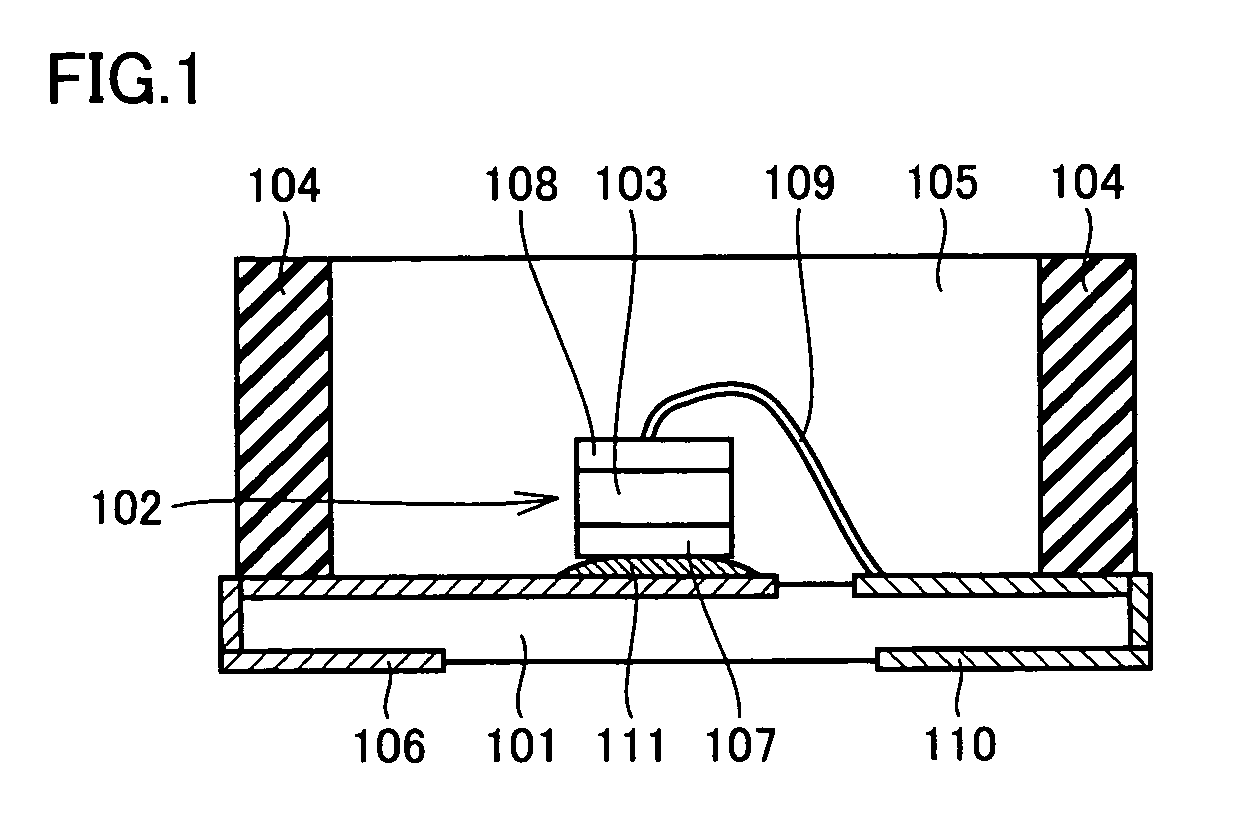
[0068]FIG. 1 is a schematic cross-sectional view of a light-emitting device according to an embodiment of the present invention. Description will be given hereinafter with reference to FIG. 1.

[0069]In the light-emitting device shown in FIG. 1, a semiconductor light-emitting element 102 is arranged on a printed wiring board 101 serving as a base. Semiconductor light-emitting element 102 preferably includes an InGaN layer 103 as an active layer as shown in FIG. 1. In addition, inside of a resin frame 104 is filled with a mold resin 105 formed of a light-transmitting resin in which a phosphor is dispersed, to seal semiconductor light-emitting element 102. In the inside of resin frame 104, an n electrode portion 106 arranged from an upper surface to a rear surface of printed wiring board 101 and an n-side electrode 107 of semiconductor light-emitting element 102 are electrically connected to each other through a conductive adhesive 111. On the other hand, a p-side electrode 108 of ...

second embodiment

vice

[0083]The light-emitting device according to another embodiment of the present invention will be described hereinafter with reference to FIG. 1. In the present embodiment, the first phosphor, the second phosphor, and a third phosphor are dispersed as the phosphor with which mold resin 105 is filled.

[0084]In the present embodiment, from a point of view of better color purity of blue light when the light-emitting device according to the present invention is used also as the backlight source, semiconductor light-emitting element 102 emitting the excitation light has the emission peak wavelength preferably in a range from 390 to 550 nm, particularly preferably in a range from 390 nm to 420 nm, and most preferably in a range from 400 nm to 410 nm. In the present embodiment, the reason why the emission peak wavelength is particularly preferably in a range from 390 nm to 420 nm is that, if the emission peak wavelength is shorter than 390 nm, energy as ultraviolet is high and hence dete...

third embodiment

evice

[0089]The light-emitting device according to another embodiment of the present invention will be described hereinafter with reference to FIG. 1. In the present embodiment, only the first phosphor is dispersed as the phosphor with which mold resin 105 is filled. Therefore, in the light-emitting device of the present embodiment, as fluorescence emitted as a result of irradiation with semiconductor light-emitting element 102 is green light, such a light-emitting device is also referred to as a green light-emitting device.

[0090]In the present embodiment, from a point of view of better color purity of blue light when the light-emitting device according to the present invention is used also as the backlight source, semiconductor light-emitting element 102 emitting the excitation light has the emission peak wavelength preferably in a range from 390 to 420 nm and most preferably in a range from 400 nm to 410 nm.

[0091]In addition, similarly, a red light-emitting device emitting red ligh...


PUM


Abstract

A method of manufacturing a first phosphor of which emission spectrum shape well matches with a color filter of three primary colors of light, a light-emitting device including the first phosphor, and an image display apparatus including the light-emitting device are provided. The light-emitting device includes a semiconductor light-emitting element emitting excitation light and the first phosphor absorbing the excitation light and emitting green light. The first phosphor contains a solid solution of aluminum element and a metal element M selected from the group consisting of Mn, Ce and Eu in crystals of an oxynitride having a β-type Si3N4 crystal structure, an amount of oxygen in the crystals being not higher than 0.8 mass %.

Description

[0001]This nonprovisional application is based on Japanese Patent Applications Nos. 2007-143745 and 2007-318468 filed with the Japan Patent Office on May 30, 2007 and Dec. 10, 2007, respectively, the entire contents of which are hereby incorporated by reference.FIELD OF THE INVENTION[0002]The present invention relates to a method of manufacturing a phosphor having a β-type Si3N4 crystal structure and emitting visible light as a result of excitation with near ultraviolet or visible light. In addition, the present invention relates to a light-emitting device suitable for a backlight source of a liquid crystal display or the like, including the phosphor manufactured with the manufacturing method, as well as to an image display apparatus including the light-emitting device.DESCRIPTION OF THE BACKGROUND ART[0003]A phosphor is used in a vacuum-fluorescent display (VFD), a field emission display (FED) or a surface-conduction electron-emitter display (SED), a plasma display panel (PDP), a c...

Claims


Application Information

Patent Timeline
IPC IPC(8): H01J1/62B05D5/06
CPCC09K11/0883C09K11/7734H01L2924/181H01L2224/48091H01L2224/73265C09K11/77348H01L2924/00012H01L2924/00014
Inventor TAKAHASHI, KOHSEIHARADA, MASAMICHIHIROSAKI, NAOTO
Owner NAT INST FOR MATERIALS SCI
Why Eureka
Try Eureka