Method for forming circuit pattern

a circuit pattern and pattern technology, applied in the field of circuit pattern formation, can solve the problems of complex inventory management, considerable management costs, and extremely difficult to alter the resistance of the resistance pattern, and achieve the effect of solving additional problems that still remain to be solved

Inactive Publication Date: 2008-12-11
MURATA MFG CO LTD
View PDF2 Cites 6 Cited by
  • Summary
  • Abstract
  • Description
  • Claims
  • Application Information

AI Technical Summary

Benefits of technology

[0047]In this case, the circuit pattern is baked while the ceramic green sheet is fired. Thus, a circuit pattern of consistent quality can be formed efficiently.
[0048]A method for forming a circuit pattern as described herein can easily provide a circuit pattern having a desired resistance.

Problems solved by technology

It is therefore extremely difficult to alter the resistance of a resistance pattern by altering the dimensions of the resistance pattern.
However, this method requires many types of resistive paste having different resistances, thus requiring complicated inventory management and considerable management costs.
However, additional problems still remain to be solved.

Method used


Image

  • Method for forming circuit pattern
  • Method for forming circuit pattern
  • Method for forming circuit pattern

Examples


embodiment 1-1

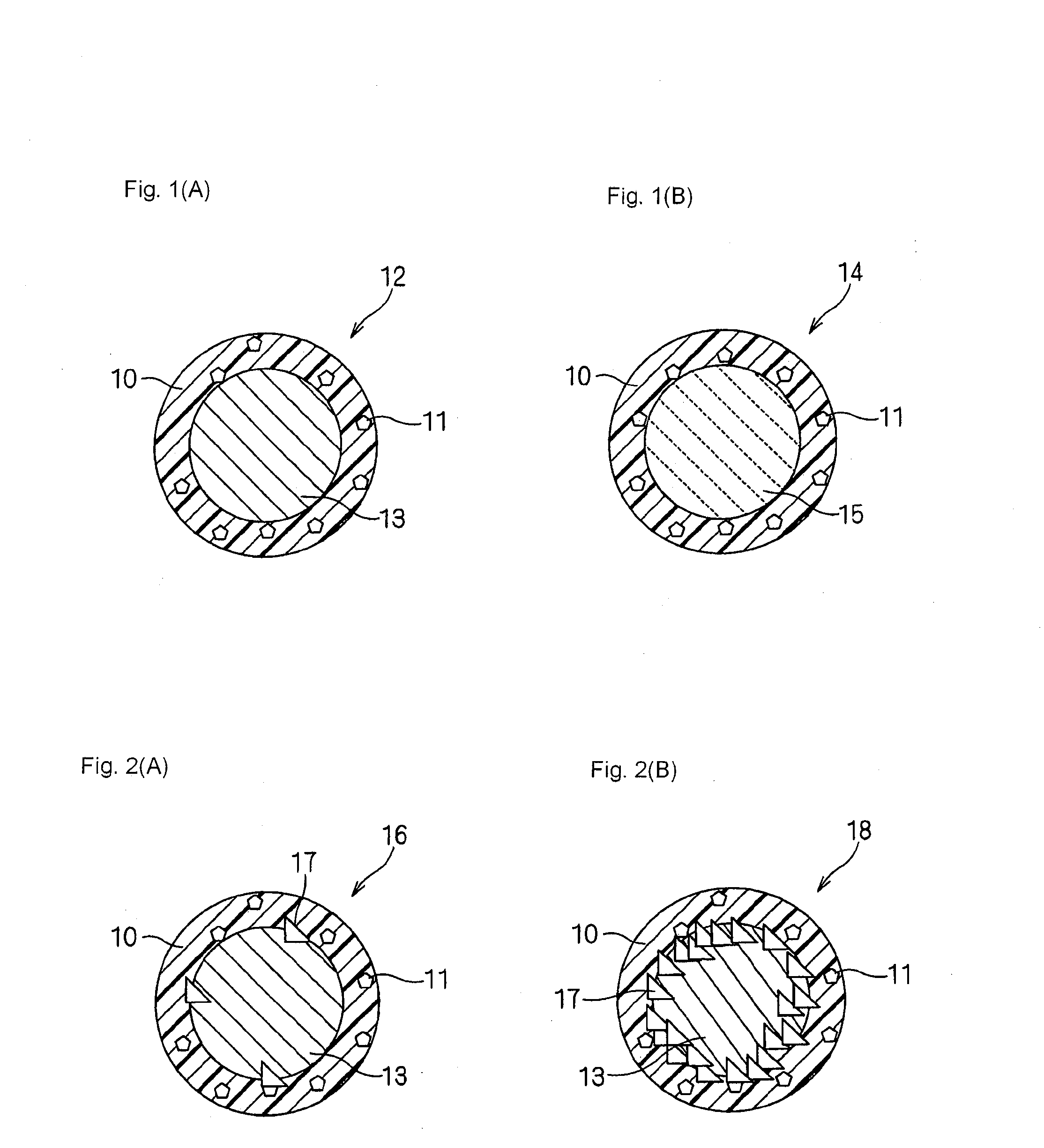
[0094]As examples of toner that have different resistances for use in the formation of a resistance pattern, FIGS. 1(A) and 1(B) schematically illustrate conductor toner 12 and glass toner 14.

[0095]As illustrated in FIG. 1(A), in the conductor toner 12, a resistor particle 13 formed of a resistive material, such as ruthenium oxide, is coated with a resin layer 10, which contains a charge control agent 11.

[0096]The conductor toner 12 may be produced as follows. First, a ruthenium oxide powder having an average particle size of 6.1 μm, a styrene acrylic resin, and an azo charge control agent are mixed in a hybridization system (Nara Machinery Co., Ltd.) at a weight ratio of 90:9.9:0.1 to produce conductor toner 12 having an average particle size of 7.3 μm. The conductor toner 12 and a ferrite carrier having an average particle size of 60 μm are mixed at a weight ratio of 20:80 to produce a developer that contains the conductor toner 12 and the ferrite carrier.

[0097]As illustrated in F...

embodiment 1-2

[0099]As other types of toner that have different resistances for use in the formation of a resistance pattern, FIGS. 2(A) and 2(B) schematically illustrate low-resistance toner 16 having a relatively low resistance and high-resistance toner 18 having a relatively high resistance, respectively.

[0100]As illustrated in FIG. 2(A), in the low-resistance toner 16, a resistor particle 13 formed of a resistive material, such as ruthenium oxide, contains glass frit 17 embedded in the surface thereof, and is coated with a resin layer 10, which contains a charge control agent 11.

[0101]The low-resistance toner 16 may be produced as follows. B2O3, SiO2, BaO, CaO, and Al2O3 are prepared as raw materials of irreducible borosilicate glass frit. These materials are mixed at a molar ratio of 36.0:31.7:18.0:9.3:5.0. The mixture is melted at a temperature in the range of 1200° C. to 1350° C. and is then quenched in pure water. The quenched mixture is pulverized with a vibrating mill into irreducible g...

embodiment 2-1

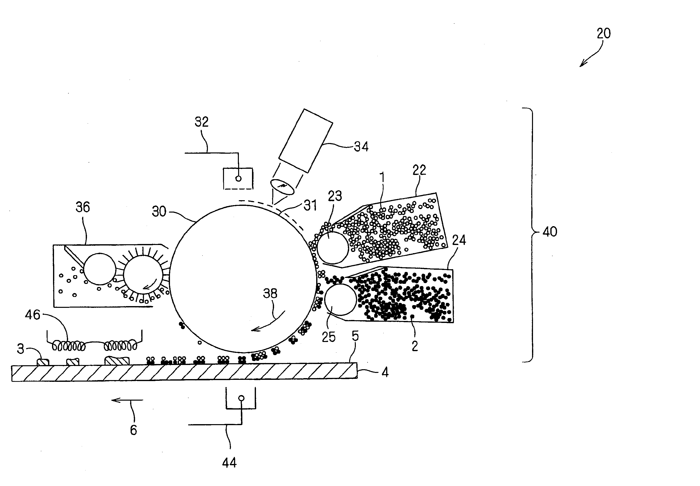
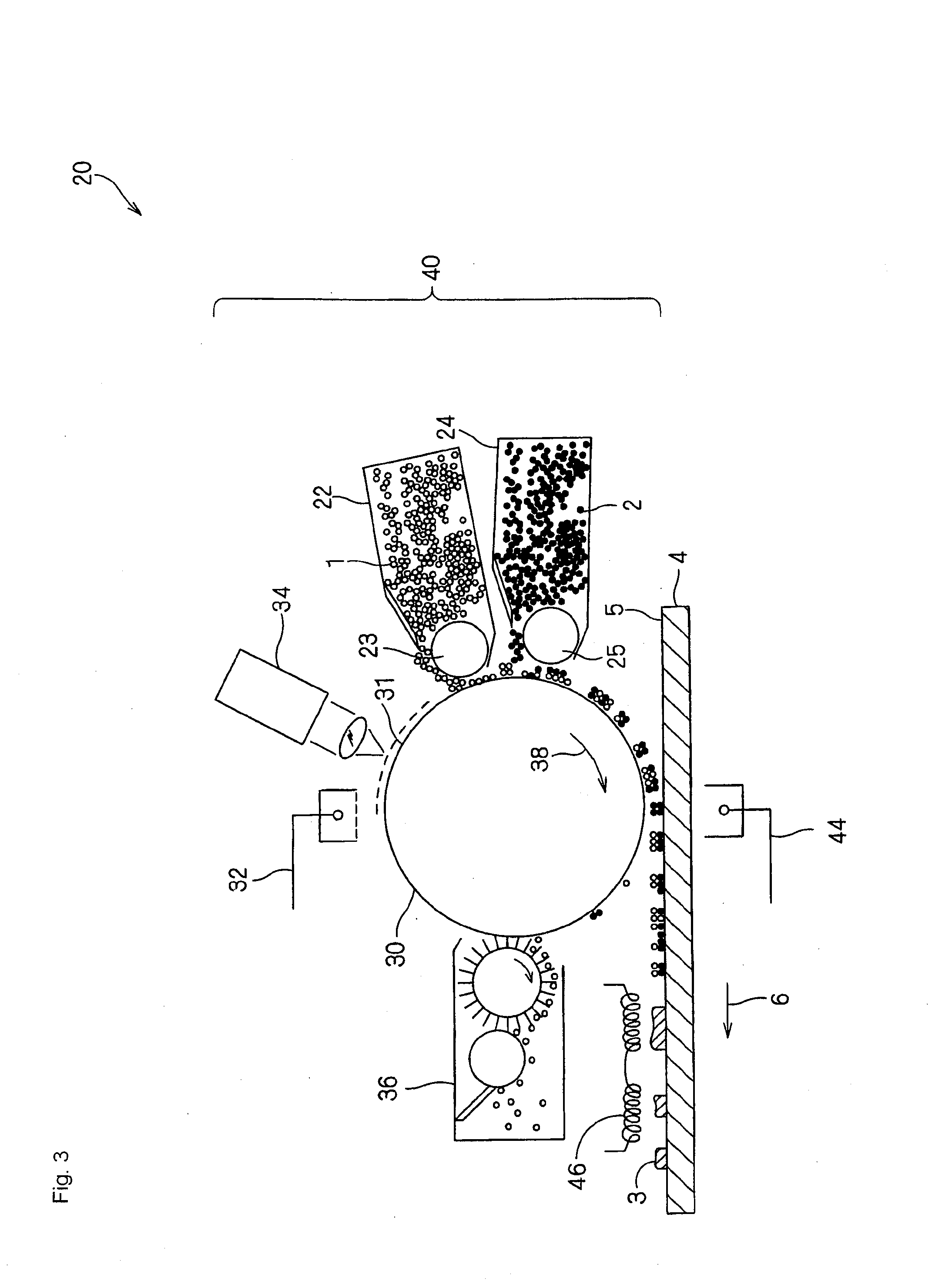
[0106]FIG. 3 schematically illustrates the structure of a single-drum-type electrophotographic apparatus 20.

[0107]The electrophotographic apparatus 20 includes an electrophotography engine unit 40, a transfer apparatus 44, and a fixing apparatus 46.

[0108]The electrophotography engine unit 40 includes a charger 32, an exposure apparatus 34, a first developing unit 22, a second developing unit 24, and a cleaner 36 each disposed around a drum-type photoreceptor 30. The charger 32 electrifies the surface 31 of the photoreceptor 30. For example, the charger 32 may be a corona charger. The exposure apparatus 34 irradiates the surface 31 of the photoreceptor 30 with light to form a desired latent image pattern (not shown). The first developing unit 22 supplies first toner 1 containing a resistive material onto the latent image pattern formed on the photoreceptor 30 to develop a first toner image. The second developing unit 24 supplies second toner 2 containing a resistive material onto the...


PUM

PropertyMeasurementUnit
particle sizeaaaaaaaaaa
weight ratioaaaaaaaaaa

Abstract

A method for forming circuit patterns having different resistances. The method includes (1) a first step of forming a first toner image using a first toner and a second toner image using a second toner, each by electrophotography, the first toner containing a resistive material, the second toner having a resistance different from that of the first toner; and (2) a second step of transferring and fixing the first toner image and the second toner image to an object to be printed such as a ceramic green sheet, to form a circuit pattern.

Description

CROSS-REFERENCE TO RELATED APPLICATIONS[0001]This is a continuation under 35 U.S.C. § 111 (a) of PCT / JP2007 / 051525 filed Jan. 30, 2007, and claims priority of JP2006-051347 filed Feb. 27, 2006, both incorporated by reference.BACKGROUND[0002]1. Technical Field[0003]The present disclosure relates to a method for forming a circuit pattern and, more particularly, to a method for forming a circuit pattern by printing, utilizing electrophotography.[0004]2. Background Art[0005]A ceramic multilayer board may include a resistance pattern serving as a resistance element and a circuit pattern including wiring serving as an inductor and / or a capacitor electrode.[0006]For example, a resistance pattern inside a ceramic multilayer board is formed by applying resistive paste to a ceramic green sheet, forming a green laminate composed of the ceramic green sheet and another ceramic green sheet, and firing the green laminate.[0007]A resistance pattern on the surface of a ceramic multilayer board is ge...

Claims


Application Information

Patent Timeline
Patent Type & Authority Applications(United States)
IPC IPC(8): G03G13/20
CPCG03G9/081H05K2203/0517G03G9/0833G03G9/08711G03G9/09725G03G9/0975G03G13/00G03G13/013H05K1/0306H05K1/092H05K1/167H05K3/102H05K3/1266H05K3/207H05K2203/0143G03G9/0823G03G15/224G03G15/6585G03G13/0139
Inventor KAMADA, AKIHIKOSAKAI, NORIOYAMAMOTO, ISSEI
Owner MURATA MFG CO LTD
Why Eureka
Try Eureka