Method and apparatus for fabricating high tensile stress film

Active Publication Date: 2008-12-11
UNITED MICROELECTRONICS CORP
View PDF6 Cites 31 Cited by
  • Summary
  • Abstract
  • Description
  • Claims
  • Application Information

AI Technical Summary

Benefits of technology

[0014]The methods for fabricating the high tensile stress film, the poly stressor, and the CESL utilize the UVRTP to cure the high tensile stress film, the poly stressor, and the CESL and simultaneously adjust the respective tensile-stress status of each. Because the tensile-stress status is adjusted by energy from a combination of photons and heat, the high tensile stre

Problems solved by technology

As semiconductor processes advance to very deep sub-micron geometries, such as 65-nm node and beyond, and with the progress of device miniaturization, enhancing carrier mobility and a driving current of a Metal-Oxide-Semiconductor (MOS) transistor has become a critical issue.
However, so far 1.5 GPa is an upper performance limit for the high tensile stress film formed by the

Method used


Image

  • Method and apparatus for fabricating high tensile stress film
  • Method and apparatus for fabricating high tensile stress film
  • Method and apparatus for fabricating high tensile stress film

Examples


Embodiment Construction

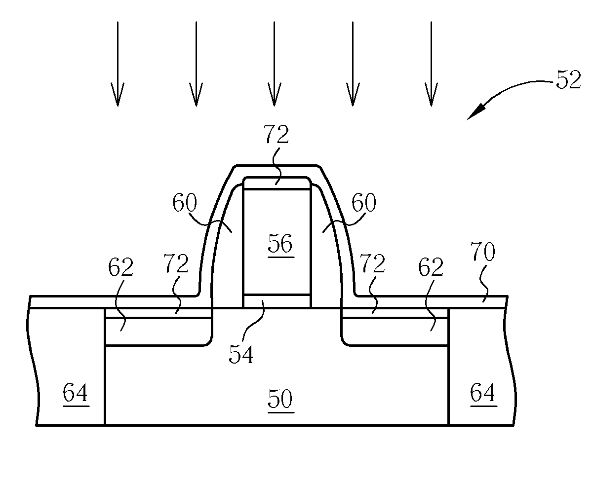
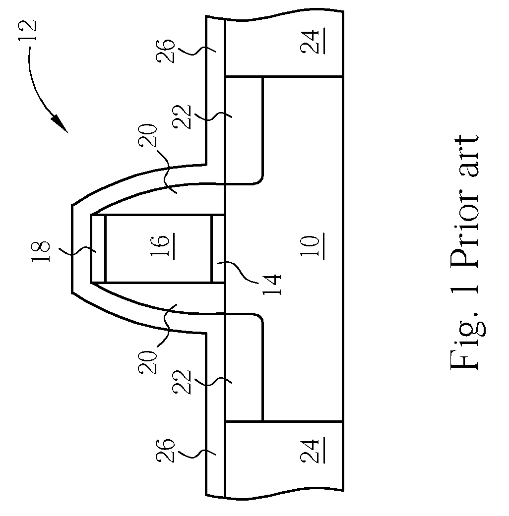
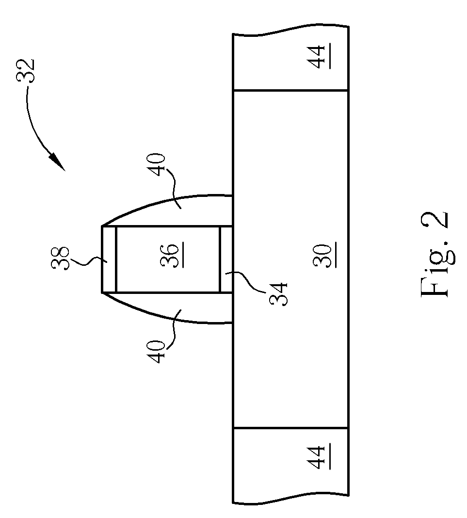
[0021]Please refer to FIGS. 2-4, which are schematic drawings illustrating the method for fabricating high tensile stress film according to a first preferred embodiment taught by the present invention. As shown in FIG. 2, a substrate 30 such as a silicon wafer or a silicon-on-insulator (SOI) substrate is provided first. The substrate 30 has at least a gate structure 32 of a transistor, such as an NMOS transistor, formed thereon, and the gate structure 32 comprises a gate dielectric 34 and a gate 36 formed on the gate dielectric 34. A cap layer 38 is formed on top of the gate 36 and an ONO offset spacer 40 is formed on sidewalls of the gate structure 32. The gate dielectric 34 composed of silicon oxide or silicon nitride is formed by a thermal oxidation or a deposition; and the cap layer 38 protecting the gate 36 is formed by silicon nitride. In addition, shallow trench isolations (STIs) 44 around the gate structure 32 are formed in the substrate 30 for electrically isolating the tra...


PUM


Abstract

A method and an apparatus for fabricating a high tensile stress film includes providing a substrate, forming a poly stressor on the substrate, and performing an ultra violet rapid thermal process (UVRTP) for curing the poly stressor and adjusting its tensile stress status, thus the poly stressor serves as a high tensile stress film. Due to a combination of energy from photons and heat, the tensile stress status of the high tensile stress film is adjusted in a relatively shorter process period or under a relatively lower temperature.

Description

BACKGROUND OF THE INVENTION[0001]1. Field of the Invention[0002]The present invention relates to a method for fabricating a high tensile stress film, and more particularly, to a method for fabricating a high tensile stress film on a strained-silicon Metal-Oxide-Semiconductor (MOS) transistor.[0003]2. Description of the Prior Art[0004]As semiconductor processes advance to very deep sub-micron geometries, such as 65-nm node and beyond, and with the progress of device miniaturization, enhancing carrier mobility and a driving current of a Metal-Oxide-Semiconductor (MOS) transistor has become a critical issue. In order to improve a speed of the MOS transistors, a strained-silicon technique has been developed and is taken as a main solution to improve performance of the MOS transistor. This technique improves scaling limits and device performance by introducing strain into the channel region, which can improve electron and hole mobility.[0005]In one approach of the strained-silicon techni...

Claims


Application Information

Patent Timeline
IPC IPC(8): H01L21/336H01J37/08
CPCH01L21/324H01L29/665H01L29/66575H01L29/78H01L29/7843
Inventor LIAO, HSIU-LIENCHEN, NENG-KUOTSAI, TENG-CHUNCHEN, YI-WEI
Owner UNITED MICROELECTRONICS CORP
Why Eureka
Try Eureka