Wiring substrate with reinforcing member

a technology of wiring substrate and reinforcing member, which is applied in the direction of printed circuit aspects, printed circuit stress/warp reduction, basic electric elements, etc., can solve the problems of increasing the external diameter, increasing the manufacturing cost of the stiffener b>105/b>, and increasing the manufacturing cost of the semiconductor package b>100/b>, so as to suppress the warpage of the resin wiring substrate 101, the effect of high stiffness of the stiffener itsel

Inactive Publication Date: 2008-12-18
NGK SPARK PLUG CO LTD
View PDF6 Cites 74 Cited by
  • Summary
  • Abstract
  • Description
  • Claims
  • Application Information

AI Technical Summary

Benefits of technology

[0006]Meanwhile, since the stiffener 105 has a simple shape (a flat plate shape) which comes into contact with only one surface of the resin wiring substrate 101, it is necessary to make the stiffness of the stiffener itself high in order to give the function to suppress the warpage of the resin wiring substrate 101. Thus, although it is conceivable to make the stiffener 105 thick, the whole semiconductor package 100 becomes thick,...

Problems solved by technology

However, since the metallic material of high stiffness is generally expensive, the manufacturing cost of the stiffener 105 will rise, and consequently the manufacturing cost of the semiconductor pack...

Method used


Image

  • Wiring substrate with reinforcing member
  • Wiring substrate with reinforcing member
  • Wiring substrate with reinforcing member

Examples


Embodiment Construction

[0085]Hereinafter, one embodiment of the invention will be described in detail with reference to the drawings.

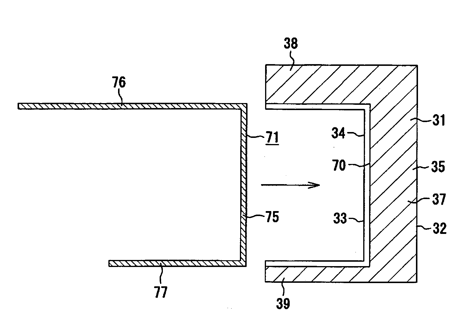
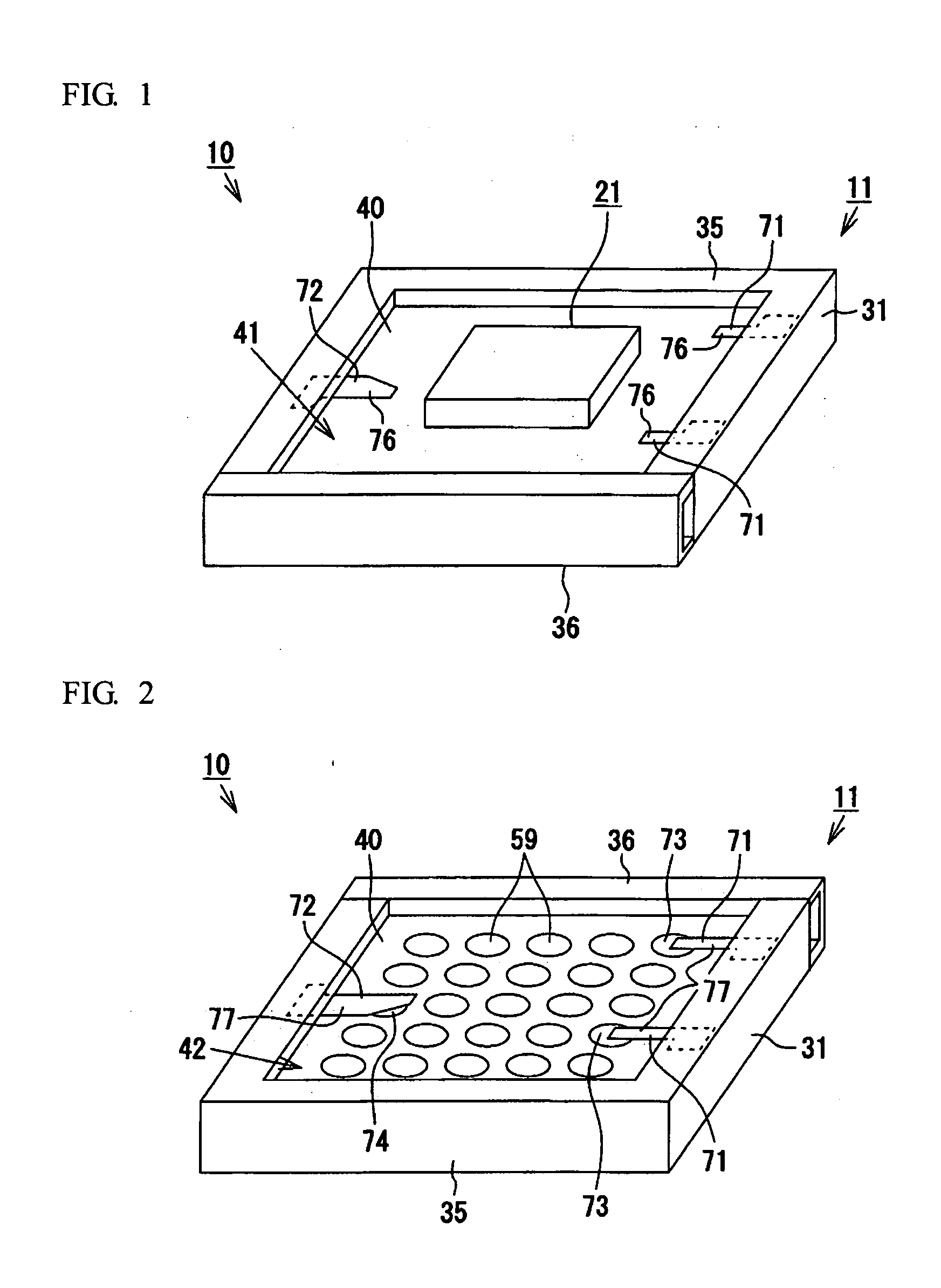
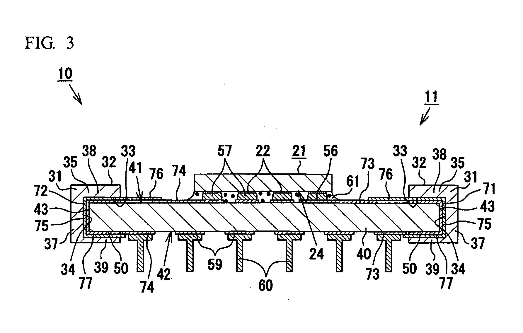
[0086]As shown in FIGS. 1 to 4, a semiconductor package 10 of this embodiment is a PGA (pin grid array) composed of a wiring substrate 11 with a stiffener (wiring substrate with a reinforcing member), and an LSI chip 21 which is a semiconductor integrated circuit element. In addition, the form of the semiconductor package 10 is not limited only to the PGA. For example, the semiconductor package may be a BGA (ball grid array), an LGA (land grid array), etc. The LSI chip 21 has a rectangular flat shape of 15.0 mm (length)×15.0 mm (width)×0.8 mm (thickness), and is made of silicon whose thermal expansion coefficient is 4.2 ppm / ° C. A circuit element which is not shown is formed on a surface layer on the side of a bottom surface 24 of the LSI chip 21. Further, a plurality of surface connection terminals 22 are provided in a grid pattern on the side of the bottom surface 24 of th...


PUM


Abstract

A wiring substrate with a reinforcing member includes: a resin wiring substrate having a substrate principal surface, a substrate rear surface, and substrate side surfaces, forming a rectangular shape having four sides in plan view, and including a resin insulating layer and a conductor layer; and a reinforcing member formed in a rectangular frame shape which surrounds the four sides of the resin wiring substrate, and provided with an inner wall having a depression surface-joined to at least one of the substrate side surfaces, an outer peripheral portion of the substrate principal surface, and an outer peripheral portion of the substrate rear surface.

Description

CROSS-REFERENCE TO RELATED APPLICATIONS[0001]This application claims the benefit of Japanese Patent Application JP 2007-158841, filed Jun. 15, 2007, and Japanese Patent Application JP 2007-158842, filed Jun. 15, 2007, the entire contents of which are hereby incorporated by reference, the same as if set forth at length.FIELD OF THE INVENTION[0002]The present invention relates to the wiring substrate with a reinforcing member including a reinforcing member for preventing the warpage of a resin wiring substrate.BACKGROUND OF THE INVENTION[0003]The spread of electronics devices like personal computers or cellular phones is bringing large changes in social structure as the IT revolution. The heart of this technique is the large-scale semiconductor integrated circuit (LSI) technique, and the operating frequency of this LSI (LSI chip) tends to become increasingly high in order to achieve the improvement in computing speed. In addition, an LSI chip is used in the state of being flip-chip co...

Claims


Application Information

Patent Timeline
IPC IPC(8): H05K1/02
CPCH01L23/49833H05K1/0271H05K1/0284H05K1/142H01L2224/73204H05K2201/2018H01L2224/16225H01L2224/16227H05K2201/2009H01L2224/05573H01L2224/05568H01L2924/00014H01L2224/05599
Inventor KAWABE, TADAHIKO
Owner NGK SPARK PLUG CO LTD
Why Eureka
Try Eureka