Video display device capable of compensating for display defects

a video display device and display defect technology, applied in the field of display devices, can solve problems such as display defects, display defects that cannot be repaired by the repair process, and deviations in parasitic capacity among thin film transistors, and achieve the effect of simple circuit configuration

Active Publication Date: 2008-12-18
LG DISPLAY CO LTD
View PDF12 Cites 36 Cited by
  • Summary
  • Abstract
  • Description
  • Claims
  • Application Information

AI Technical Summary

Benefits of technology

[0011]An object of embodiments of the invention is to provide a video display device capable of compensating for various display defects using compensation data and having a simple circuit configuration.

Problems solved by technology

However, there may be display defects that cannot be repaired by the repair process.
Display defects are mainly caused by a deviation in the amount of light exposure from overlapped light exposure in a multi-exposure operation of exposure equipment used in a thin film pattern formation process or from aberrations of the multi-lenses used in the exposure equipment.
More specifically, a deviation in the amount of light exposure causes a variation in the width of thin film patterns, thereby resulting in deviation in parasitic capacity among thin film transistors, deviation in height among column spacers for maintaining a desired cell gap, and / or a deviation in parasitic capacity among signal lines.
Such deviations cause brightness aberrations appearing as display defects.
However, it is difficult, if not impossible, to eliminate all such vertical or horizontal-line-shaped display defects through improvements in the processing techniques.
Although such defective pixels are subjected to a repair process, they can still have point defects in the repaired state.
Also, when a repair process is performed such that the pixel repaired in the form of a dark pixel is linked to a neighboring normal pixel, the linked pixels may be displayed as point defects due to a shortage of data charge amount because data supplied to the normal pixel must also be distributed evenly to the repaired pixel.
However, the related art circuit-based compensation methods have problems in using a horizontal line data compensation circuit to address a display device having vertical line display defects, and, vice versa, to apply a vertical line data compensation circuit to a display device having horizontal line display defects.
Related art circuit-based compensation methods also can not achieve adaptive addition and subtraction of a compensation value in accordance with the brightness of an associated defect region.
For example, there is a problem in that it is difficult to quantify and systematize compensation values for defect regions by using a method, in which a defect region is compensated for brightness such that the defect region becomes brighter than normal regions around the defect region, on the assumption that the defect region is dark, or a method, in which, when the defect region is bright, the normal regions are compensated for brightness such that the normal regions become brighter.

Method used


Image

  • Video display device capable of compensating for display defects
  • Video display device capable of compensating for display defects
  • Video display device capable of compensating for display defects

Examples


first embodiment

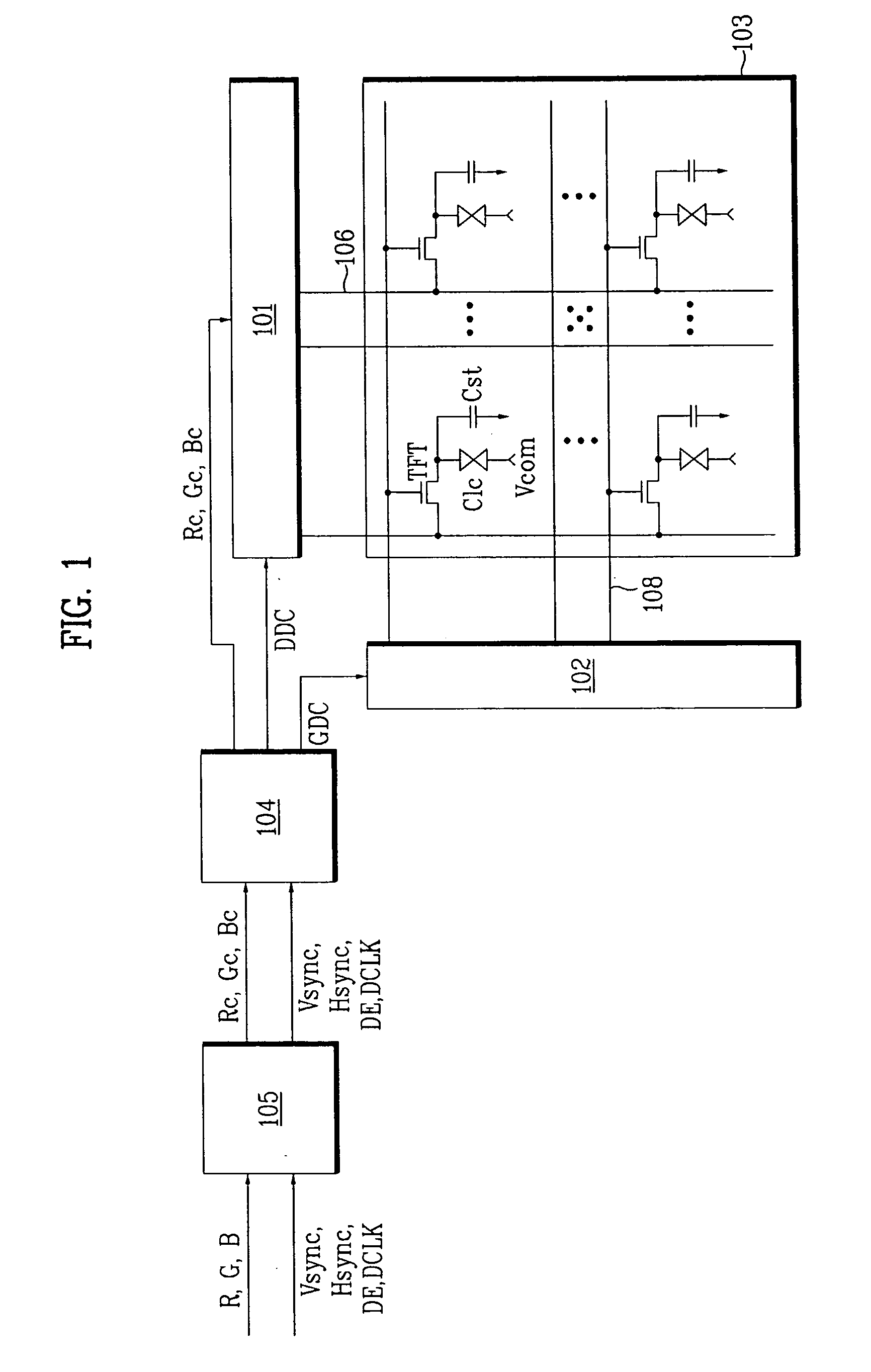
[0048]FIG. 8 illustrates a data compensation circuit of the LCD device according to the invention. As shown in FIG. 8, the data compensation circuit 105 includes a memory 40 storing typical defect information and point defect information, a first compensator 30 for compensating data Re, Ge, and Be of a typical defect region, using the typical defect information stored in the memory 40, and outputting data Rm1, Gm1, and Bm1 as compensated data, a second compensator 160 for finely compensating data Rm1, Gm1, and Bm1 output from the first compensator 30 by spatially and temporally distributing the data Rm1, Gm1, and Bm1, using an FRC dithering method, and a third compensator 170 for compensating data of a point defect region, using the point defect information stored in the memory 40. The third compensator 170 is coupled to the second compensator 160. For data of normal regions, the data compensation circuit 105 outputs the data without any data compensation.

[0049]As described above, t...

second embodiment

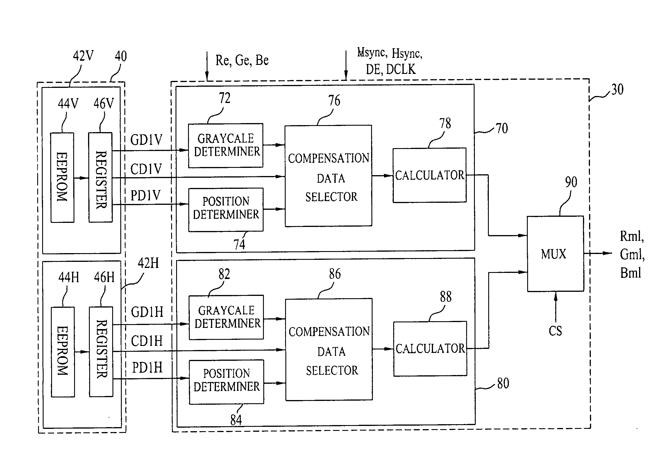
[0083]FIG. 13 illustrates a data compensation circuit of the LCD device according to the invention. As shown in FIG. 13, the data compensation circuit includes a memory 100 storing typical defect information PD1, CD1, and GD1 and point defect information PD2, CD2, and GD2, a first compensator 110 for compensating data Re, Ge, and Be of a typical defect region, using the typical defect information PD1, CD1, and GD1 stored in the memory 100, and outputting data Rm1, Gm1, and Bm1 as compensated data, a second compensator 160 for finely compensating data Rm1, Gm1, and Bm1 output from the first compensator 110 by spatially and temporally distributing the data Rm1, Gm1, and Bm1, using an FRC dithering method, and a third compensator 170 for compensating data of a point defect region, using the point defect information PD2, CD2, and GD2 stored in the memory 100. The third compensator 170 is coupled to the second compensator 160.

[0084]The first compensator 110 shown in FIG. 13 is different ...

third embodiment

[0110]FIG. 17 illustrates a data compensation circuit of the LCD device according to the invention. As shown in FIG. 17, the data compensation circuit includes a memory 100 storing typical defect information PD1, CD1, and GD1 and point defect information PD2, CD2, and GD2, a first compensator 220 for compensating data Re, Ge, and Be of a typical defect region, using the typical defect information PD1, CD1, and GD1 stored in the memory 100, and outputting data Rm1, Gm1, and Bm1 as compensated data, a second compensator 160 for finely compensating data Rm1, Gm1, and Bm1 output from the first compensator 220 by spatially and temporally distributing the data Rm1, Gm1, and Bm1, using an FRC dithering method, and a third compensator 170 for compensating data of a point defect region, using the point defect information PD2, CD2, and GD2 stored in the memory 100. The third compensator 170 is coupled to the second compensator 160.

[0111]The first compensator 220 shown in FIG. 17 is different ...


PUM


Abstract

A video display device capable of compensating for display defects, comprising: liquid crystal panel for displaying an image through a pixel matrix; a data driver for outputting data to data lines of the liquid crystal display panel; a gate driver for driving the gate lines of the liquid crystal display panel; a timing controller for receiving compensated data, uncompensated data and synchronizing signals to output a gate control signal to the gate driver and to output both resultant data and a data control signal to the data driver; and a memory for storing information on point defect information on the liquid crystal display panel, and at least one of horizontal and vertical line defects of the liquid crystal display panel of the liquid crystal display panel; and a data compensation circuit for receiving display data and synchronizing signals, and outputting compensated data to the timing controller based on the information in the memory and uncompensated data to the timing controller, wherein the data compensation circuit includes a vertical line compensator for compensating a vertical line defect of the liquid crystal display panel, a horizontal line compensator for compensating a horizontal line defect of the liquid crystal display panel, and a multiplexer for selecting an output from one of the vertical line compensator and the horizontal line compensator in accordance with whether a defect is a vertical line defect or a horizontal line defect.

Description

[0001]This application claims the benefit of the Korean Patent Application No. P2007-058492 filed on Jun. 14, 2007, Korean Patent Application No. P2007-111217 filed on Nov. 1, 2007, Korean Patent Application No. P2008-014842 filed Feb. 19, 2008 and Korean Patent Application No. P2008-030827 filed Mar. 30, 2008, which are all hereby incorporated by reference as if fully set forth herein.BACKGROUND OF THE INVENTION[0002]1. Field of the Invention[0003]Embodiments of the invention relate to a display device, and more particularly, to a video display device capable of compensating for display defects. Although embodiments of the invention are suitable for a wide scope of applications, they are particularly suitable for using compensation data to achieve an enhancement in display quality.[0004]2. Discussion of the Related Art[0005]Recently, for video display devices, flat display devices, such as liquid crystal display (LCD), plasma display panel (PDP), and organic light emitting diode (O...

Claims


Application Information

Patent Timeline
Patent Type & Authority Applications(United States)
IPC IPC(8): G09G3/36
CPCG09G3/006G09G3/2055G09G2330/10
Inventor HWANG, JONG HEE
Owner LG DISPLAY CO LTD
Why Eureka
Try Eureka