Photomask manufacturing method and semiconductor device manufacturing method

a manufacturing method and semiconductor technology, applied in the direction of photomechanical equipment, instruments, originals for photomechanical treatment, etc., can solve the problems of insufficient reflection coefficient of reflective mask, inability to accurately correct the pattern dimensions of reflective mask, and change the transmittance of transparent mask

Active Publication Date: 2008-12-18
KIOXIA CORP
View PDF5 Cites 20 Cited by
  • Summary
  • Abstract
  • Description
  • Claims
  • Application Information

AI Technical Summary

Problems solved by technology

However, using this technique, the transmittance of the transparent mask may be changed, while the reflection coefficient of the reflective mask cannot be sufficiently changed.
As a r...

Method used


Image

  • Photomask manufacturing method and semiconductor device manufacturing method
  • Photomask manufacturing method and semiconductor device manufacturing method
  • Photomask manufacturing method and semiconductor device manufacturing method

Examples


first embodiment

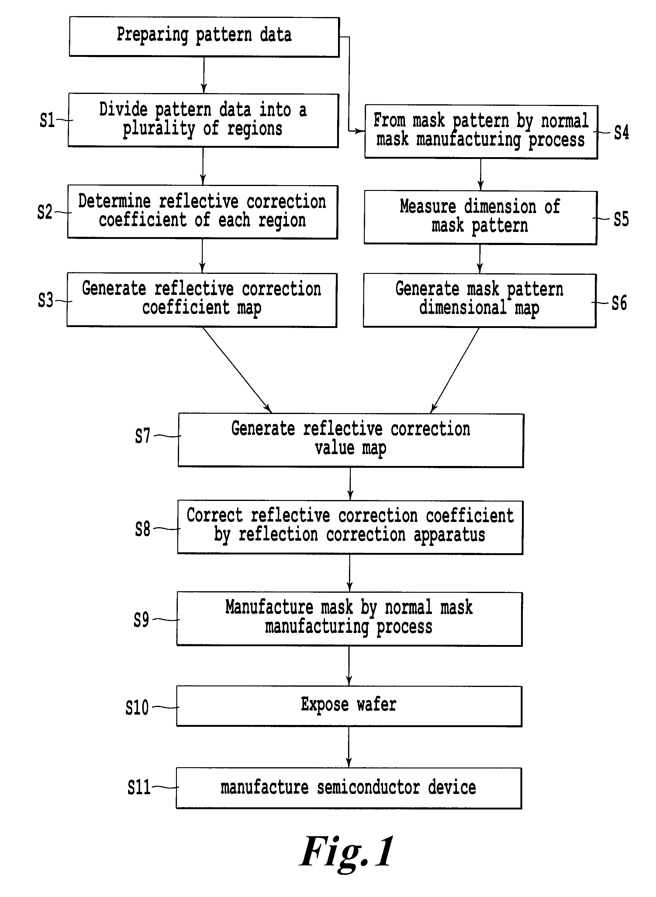
[0019]FIG. 1 is a flowchart for explaining a method of manufacturing a photomask (EUV mask) used in an EUV lithography process according to the present invention. FIG. 1 shows a process until a semiconductor device is manufactured from photomask manufacturing.

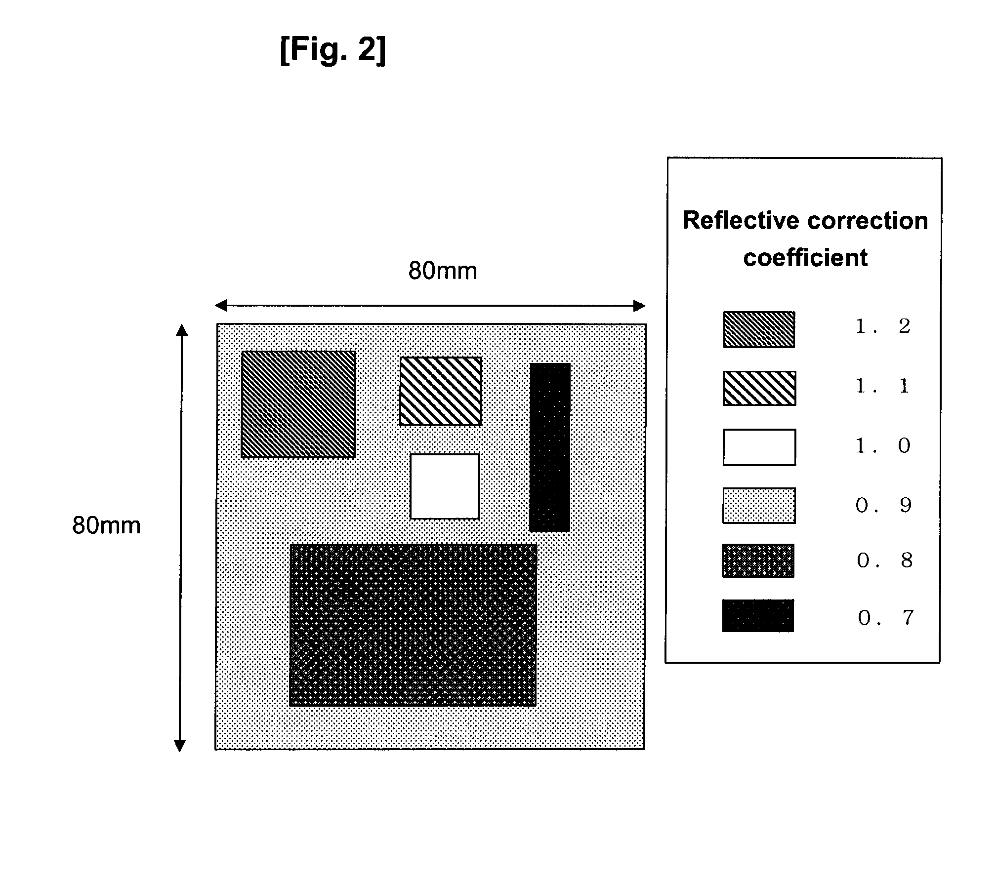
[0020]The flowchart of FIG. 1 shows steps S1-S11 performed in the process of manufacturing a semiconductor device. The steps S4-S6 have been known to be performed in a background mask manufacturing process, and result in generating a mask pattern dimensional map, discussed in further detail below. The applicants of the present invention recognized that in-plane uniformity of mask pattern dimensions can be improved by utilizing additional information than in steps S4-S6, to lead to improvements in semiconductor device manufacturing yield. Specifically, in features in the present invention a reflective correction coefficient map such as shown in FIG. 2 is generated by steps S1-S3 in FIG. 1, performed in parallel with steps S4-S6,...

third embodiment

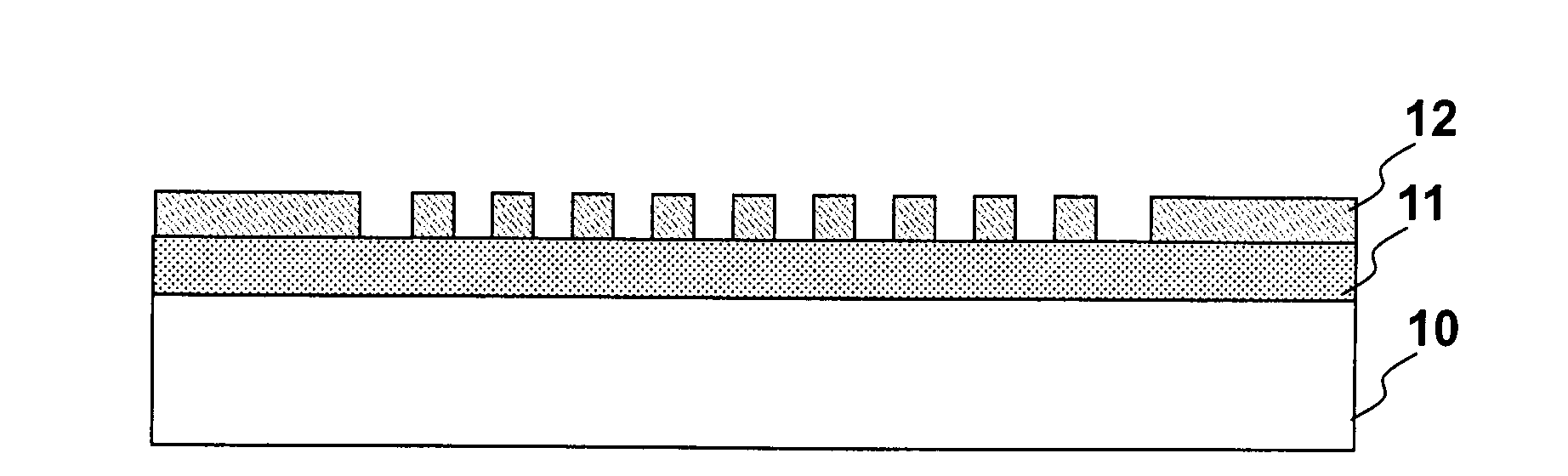
[0039]In the third embodiment, as shown in FIG. 3(b′), reflection correction is performed by implanting ions 18 into the reflective layer 11 and forming an ion implanted layer 19, according to the reflection correction coefficient map which is generated (in steps S7 or S18) based on the reflection correction coefficient map (generated in steps S3 or S14) and the pattern dimensional map (generated in steps S6 or S17). An ion implantation apparatus used in this implanting of ions for example has a variable aperture that adjusts a size of an ion implanted region. In this embodiment, the aperture in the apparatus is controlled to adjust the size of an ion implanted region in one shot for each 1 mm-square pattern data region, when the ion implantation is being performed.

[0040]For example, the implanted ions 18 are Mo ions. The ion implantation amount is changed for each 1 mm-square region in the range from 2×10¹⁴ to 5×10¹⁴ ions / cm2 to decrease the reflection coefficient by following the ...


PUM


Abstract

A photomask manufacturing method. A pattern dimensional map is generated by preparing a photomask in which a reflective layer formed on a substrate and an absorber pattern is formed on the layer. A reflection correction coefficient map is generated by dividing a mask region, where the absorber pattern is formed, into a plurality of subregions, and determining a reflection correction coefficient for each subregion. The reflection correction value of each subregion is calculated based on the dimensional difference indicated in the pattern dimensional map and the reflection correction coefficient of each subregion. A reflection coefficient of each reflective layer region corresponding to each subregion is changed based on the reflection correction value.

Description

CROSS-REFERENCE TO RELATED APPLICATIONS[0001]This application is based upon and claims the benefit of priority from the prior Japanese Patent Application No. 2007-25977, filed Feb. 5, 2007, the entire contents of which are incorporated herein by reference.BACKGROUND OF THE INVENTION[0002]1. Field of the Invention[0003]The present invention relates to a method of manufacturing a photomask including an absorber pattern on a reflective layer and, more particularly, to a method of manufacturing a photomask in a part of which the reflection coefficient of the absorber layer is changed. The present invention also relates to a semiconductor device manufacturing method using a photomask manufactured by this method.[0004]2. Description of the Background Art[0005]Along with the recent advance in the micropatterning of semiconductor devices, a demand for patterning with an EUV (Extreme Ultra Violet) lithography process has been increasing. The design rule of leading-edge devices has already re...

Claims


Application Information

Patent Timeline
IPC IPC(8): G03F1/00G03F7/20G03F1/22G03F1/24H01L21/027
CPCB82Y10/00B82Y40/00G03F1/144G03F1/24G03F1/36
Inventor ITOH, MASAMITSU
Owner KIOXIA CORP
Why Eureka
Try Eureka