Manufacturing method of semiconductor device

a manufacturing method and semiconductor technology, applied in the direction of coatings, transistors, chemical vapor deposition coatings, etc., can solve the problems of titanium film and titanium nitride film peeling, etc., to improve the operation rate of multi-chamber film forming apparatus

Active Publication Date: 2008-12-18
RENESAS ELECTRONICS CORP
View PDF54 Cites 39 Cited by
  • Summary
  • Abstract
  • Description
  • Claims
  • Application Information

AI Technical Summary

Benefits of technology

[0021]Advantages available by the typical inventions, of the inventions disclosed by the present application, will next be described briefly.
[0022]The present invention makes it possible to avoid an inconvenience at a coupling portion between a barrier metal film obtained by stacking a titanium nitride film over a titanium ...

Problems solved by technology

The barrier metal film obtained by depositing a titanium nitride film on a titanium film and thus having a film stack structure has, however, various technological problems as will be described below.
This results in a rise in contact resistance between the plug and nickel silicide layer.
In additio...

Method used


Image

  • Manufacturing method of semiconductor device
  • Manufacturing method of semiconductor device
  • Manufacturing method of semiconductor device

Examples


Embodiment Construction

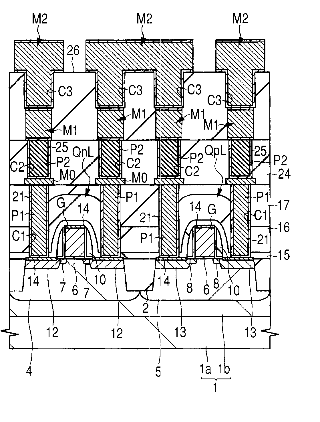
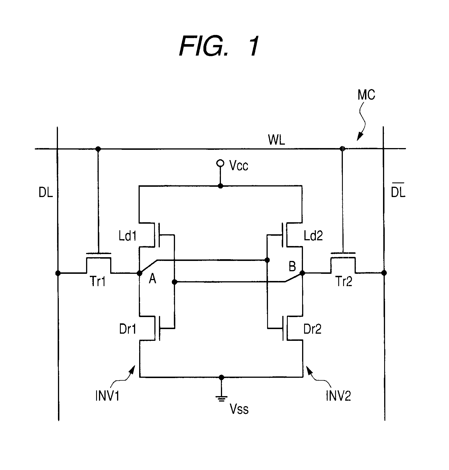
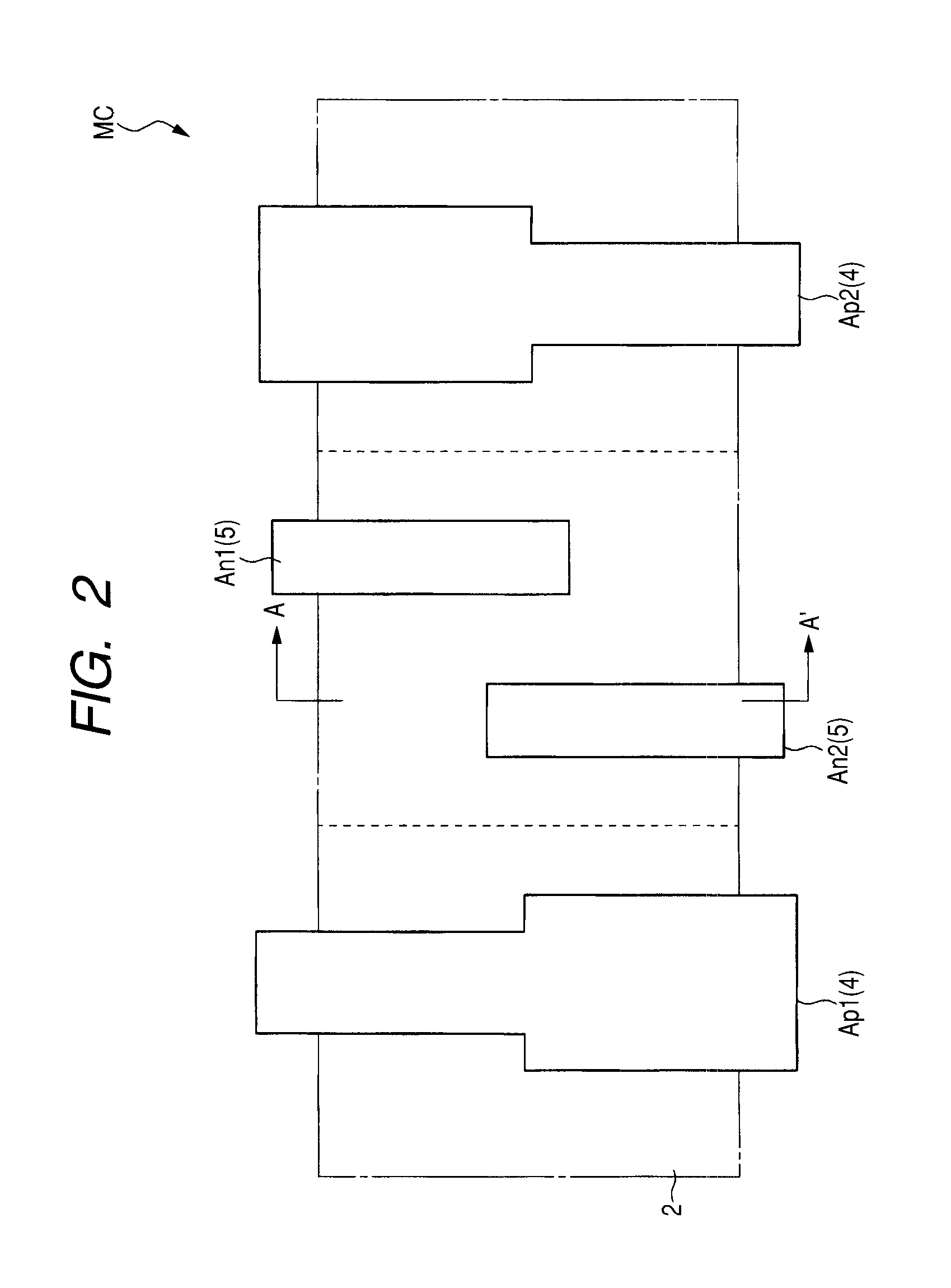
[0052]In the below-described embodiments, a description will be made after divided in plural sections or in plural embodiments if necessary for convenience's sake. These plural sections or embodiments are not independent each other, but in a relation such that one is a modification example, details or complementary description of a part or whole of the other one unless otherwise specifically indicated. In the below-described embodiments, when a reference is made to the number of elements (including the number, value, amount and range), the number of elements is not limited to a specific number but can be greater than or less than the specific number unless otherwise specifically indicated or in the case it is principally apparent that the number is limited to the specific number. Moreover in the below-described embodiments, it is needless to say that the constituting elements (including element steps) are not always essential unless otherwise specifically indicated or in the case wh...


PUM

PropertyMeasurementUnit
Temperatureaaaaaaaaaa
Timeaaaaaaaaaa
Timeaaaaaaaaaa

Abstract

The present invention is to possible to avoid an inconvenience at a coupling portion between a barrier metal film obtained by depositing a titanium nitride film on a titanium film and thus having a film stack structure and a metal film filled, via the barrier metal film, in a connecting hole opened in an insulating film. The manufacturing method of a semiconductor device includes the steps of: forming a contact hole and exposing a nickel silicide layer from the bottom of the contact hole; forming a thermal reaction Ti film by a thermal reaction using a TiCl4 gas, forming a plasma reaction Ti film by a plasma reaction using a TiCl4 gas, carrying out plasma treatment with an H2 gas to decrease the chlorine concentration of the plasma reaction Ti film and at the same time to reduce an oxide film on the surface of the nickel silicide layer; forming a nitrogen-rich TiN film over the surface of the plasma reaction Ti film and at the same time reducing the oxide film on the surface of the nickel silicide layer by thermal nitridation treatment with an NH3 gas and plasma treatment with an NH3 gas.

Description

CROSS-REFERENCE TO RELATED APPLICATIONS[0001]The disclosure of Japanese Patent Application No. 2007-158238 filed on Jun. 15, 2007 including the specification, drawings and abstract is incorporated herein by reference in its entirety.BACKGROUND OF THE INVENTION[0002]The present invention relates to a manufacturing technology of a semiconductor device, in particular, to a technology effective when applied to a manufacturing step of a semiconductor device for filling a metal film, via a barrier metal film, in a connecting hole opened in an insulating film.[0003]Japanese Patent Laid-Open No. 2004-363402 discloses a method of forming a Ti layer on at least the inner wall and bottom portion of a contact hole penetrating an insulating layer, nitriding the Ti layer with N radicals to form a TiN layer on the Ti layer, and filling a conductive layer in the contact hole (refer to Japanese Patent Laid-Open No. 2004-363402, Paragraphs [0026] to [0028], FIGS. 4 and 5).[0004]Japanese Patent Laid-O...

Claims


Application Information

Patent Timeline
IPC IPC(8): H01L21/336
CPCC23C16/0281C23C16/14C23C16/34C23C16/4554H01L27/1104H01L21/28518H01L21/28556H01L21/76846H01L27/11C23C16/45542H01L21/76895H01L21/76897H01L21/76876H01L21/76877H10B10/00H10B10/12
Inventor FUTASE, TAKUYA
Owner RENESAS ELECTRONICS CORP
Why Eureka
Try Eureka