

Semiconductor substrate and maehtod for manufacturing the same
a technology of semiconductor devices and substrates, applied in the direction of semiconductor devices, electrical equipment, transistors, etc., can solve the problems of time and cost, single-crystal silicon substrates are likely to be damaged, etc., and achieve the effect of improving the reliability of semiconductor device manufacturing and good electric characteristics
- Summary
- Abstract
- Description
- Claims
- Application Information
AI Technical Summary
Benefits of technology
Problems solved by technology
Method used
Image

Examples
embodiment mode 1
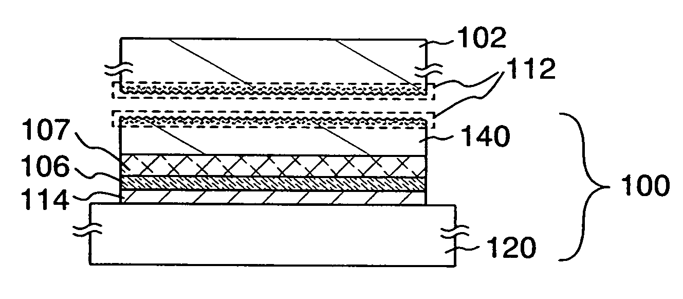
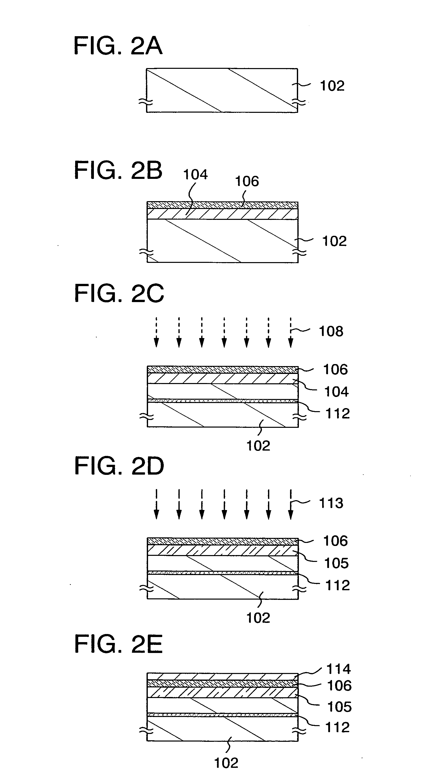
[0044]A semiconductor device manufacturing substrate of this embodiment mode has an SOI structure and is formed by transfer of a semiconductor film separated from a semiconductor substrate to a supporting substrate. As the supporting substrate, a substrate which is different from a substrate used as the semiconductor substrate is used. One mode of the semiconductor device manufacturing substrate of this embodiment mode is shown in FIG. 1.
[0045]As for a semiconductor device manufacturing substrate 100 shown in FIG. 1, a semiconductor film 140 is provided over a supporting substrate 120. An insulating film 107 containing silicon and oxygen as its composition which is in contact with the semiconductor film 140, an insulating film 106 containing silicon and nitrogen as its composition which is in contact with the insulating film 107 containing silicon and oxygen as its composition, and a bonding layer 114 which is in contact with the insulating film 106 containing silicon and nitrogen a...
embodiment mode 2
[0133]In this embodiment mode, an example of manufacturing a semiconductor device with use of a semiconductor device manufacturing substrate of the present invention will be described with reference to FIGS. 11A to 11D and FIGS. 12A and 12B.
[0134]A semiconductor device manufacturing substrate is prepared (see FIG. 11A). In this embodiment mode, an example of using the semiconductor device manufacturing substrate which has an SOI structure shown in FIG. 1, in which the semiconductor film 140 is bonded to the supporting substrate 120 with the bonding layer 114, the insulating film 106 containing silicon and nitrogen as its composition, and the third insulating film 107 containing silicon and oxygen as its composition which are stacked in order over the supporting substrate 120 interposed therebetween, is described. Note that there is no particular limitation on the structure of the semiconductor device manufacturing substrate of the present invention, and a semiconductor device manufa...
embodiment mode 3
[0152]In this embodiment mode, an example of manufacturing a semiconductor device with use of a semiconductor device manufacturing substrate of the present invention will be described with reference to FIGS. 7A to 7E, FIGS. 8A to 8C, FIGS. 9A and 9B, and FIGS. 10A and 10B. In this embodiment mode, an example of manufacturing an electroluminescence (EL) display device will be described.
[0153]A semiconductor device manufacturing substrate is prepared (see FIG. 7A). In this embodiment mode, an example of using a semiconductor device manufacturing substrate which has an SOI structure in which the semiconductor film 140 is bonded to the supporting substrate 120 with the barrier film 122, the bonding layer 124, the bonding layer 114, the insulating film 106 containing silicon and nitrogen as its composition, and the third thermal oxide film 155 which are stacked in order over the supporting substrate 120 interposed therebetween is described. The semiconductor device manufacturing substrat...
PUM
| Property | Measurement | Unit |
|---|---|---|
| temperature | aaaaa | aaaaa |
| thickness | aaaaa | aaaaa |
| thickness | aaaaa | aaaaa |
Abstract
Description
Claims
Application Information